Comparators and Waveform Generator MCQ [Free PDF] – Objective Question Answer for Comparators and Waveform Generator Quiz

71. Which circuit converts irregularly shaped waveforms to regular shaped waveforms?

A. Schmitt trigger
B. Voltage limiter
C. Comparator
D. None of the mentioned

Answer: A

Schmitt triggers are also called squaring circuits because this type of circuit converts an irregularly shaped wave to a square wave or pulse.


72. Determine the upper and lower threshold voltage

Determine the upper and lower threshold voltage

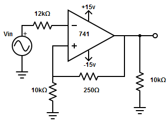
A. VUT  = +14.63v, VLT = +14.63v
B. VUT  = -14.63v, VLT = -14.63v
C. VUT  = VLT = ±14.63v
D. None of the mentioned

Answer: B

Upper threshold voltage

VUT  = [R1/(R1+ R2)]× (+Vsat)

= [10 kΩ/(10 kΩ +250Ω)]×(+15v) = +14.63v.

Lower threshold voltage

VLT  = [R1/(R1+ R2)]×( -Vsat)

= [10 kΩ /(10 kΩ+250Ω)]×(-15v) = -14.63v.


73. What happens if the threshold voltages are made longer than the noise voltages in the Schmitt trigger?

A. All the mentioned
B. Enhance the output signal
C. Reduce the transition effect
D. Eliminate false output transition

Answer: D

In the Schmitt trigger, if the threshold voltage VUT and VLT are made larger than the input noise voltage. The positive feedback will eliminate the false output transition.


74. To a Schmitt trigger in a non-inverting configuration an input triangular wave of 1Vp is applied. What will be the output waveform, if the upper and lower threshold voltages are 0.25v?

A. Square waveform
B. Pulse waveform
C. Sawtooth waveform
D. Cannot be determined

Answer: A

To a Schmitt trigger in a non-inverting configuration, an input triangular wave of 1Vp is applied. The output waveform will be a square waveform.

The input waveform has a threshold level of ±0.25v.


75. In which configuration a dead band condition occurs in the Schmitt trigger?

A. Differential amplifier with positive feedback
B. Voltage follower with positive feedback
C. Comparator with positive feedback
D. None of the mentioned

Answer: C

The comparator with positive feedback is said to exhibit hysteresis, a dead band condition when the input of the comparator exceeds the upper threshold voltage. At this condition, the output switches from +Vsat to -Vsat. It reverts back to its original state, +Vsat when the input goes below the lower threshold voltage.


76. Calculate the hysteresis voltage for the schmitt trigger from the given specification:

R2  = 56 kΩ , R1  = 100Ω ,Vref  = 0v & Vsat = ±14v.
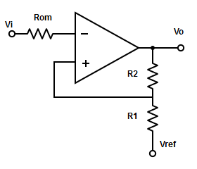
Calculate the hysteresis voltage for the schmitt trigger from the given specification:

A. 0 mv
B. 25 mv
C. 50 mv
D. -25 mv

Answer: C

Upper threshold voltage

VUT  = [R1/(R1+R2)]×( +Vsat)

= [100 kΩ/(56 kΩ +100 Ω)]×(+14v) = +25mv.

Lower threshold voltage VLT

= [R1/(R1+ R2)]×(-Vsat)

= [100 kΩ /(56 kΩ+100Ω)]×(-14v) = -25 mv.

∴ Hysteresis voltage = VUT-VLT  = 25-(-25) = 50mv.


77. How to limit the output voltage swing only to a positive direction?

A. Combination of two Zener diodes
B. Combination of Zener and rectifier diode
C. All of the mentioned
D. Combination of two rectifier diodes

Answer: B

To limit the output voltage swing to a positive or negative direction, the basic op-amp comparator should be connected with a combination of Zener and rectifier diode in the feedback path.


78. A basic op-amp circuit has a Zener and rectifier diode connected in the feedback path. Calculate the maximum positive voltage. Where, Zener voltage = 5.1 v and voltage drop across the forward-biased Zener = 0.7v?

A. VO  = 5.8v
B. VO  = 9.9v
C. VO  = 4.7v
D. VO  = 7.1v

Answer: D

Initially, the rectifier diode will be reverse biased and makes the op-amp operate in an open-loop configuration. So, the output voltage is obtained till the rectifier diode is forward bias and Zener goes into avalanche condition. Hence, the maximum positive output voltage

VO = Vz +VD (VD –> voltage drop across rectifier diode).

= > VO = 5.1v+0.7 v = 5.8v.


79. The specially designed comparators are compatible with

A. RTL
B. MOS Logic
C. TTL
D. All of the mentioned

Answer: D

The specially designed comparator outperforms the op-amp type. They are optimized for the most desirable promoters like speed and accuracy. So, their output is compatible with RTL, DTL, TTL, and MOS Logic.


80. Response time of comparators is defined as

A. Time interval between input and output crossing upper threshold voltage
B. Time interval between input and output function
C. Time interval between input and output crossing threshold logic
D. Time interval between input and output crossing lower threshold voltage

Answer: C

The response time of the comparator is the interval between the application of an input step function and the time output crosses the logic threshold voltage.

Scroll to Top