1. A Differential Amplifier should have the collector resistor’s value (RC1 & RC2) as
A. 5kΩ, 5kΩ
B. 5Ω, 10kΩ
C. 5Ω, 5kΩ
D. 5kΩ, 10kΩ
2. A Differential Amplifier amplifies
A. Input signal with higher voltage
B. Input voltage with smaller voltage
C. Sum of the input voltage
D. None of the Mentioned
3. The value of emitter resistance in Emitter Biased circuit are RE1=25kΩ & RE2=16kΩ. Find RE
A. 9.756kΩ
B. 41kΩ
C. 9.723kΩ
D. 10kΩ
4. If the output is measured between two collectors of transistors, then the Differential amplifier with two input signals is said to be configured as
A. Dual Input Balanced Output
B. Dual Input Unbalanced Output
C. Single Input Balanced Output
D. Dual Input Unbalanced Output
5. A differential amplifier is capable of amplifying
A. DC input signal only
B. AC input signal only
C. AC & DC input signal
D. None of the Mentioned
6. In an ideal Differential Amplifier, if the same signal is given to both inputs, then the output will be
A. Same as input
B. Double the input
C. Not equal to zero
D. Zero
7. An emitter bias Dual Input Balanced Output differential amplifier has VCC=20v, β=100, VBE=0.7v, RE=1.3kΩ. Find IE
A. 7.42mA
B. 9.8mA
C. 10mA
D. 8.6mA
8. Find IC, given VCE=0.77v, VCC=10v, VBE=0.37v and RC=2.4kΩ in Dual Input Balanced Output differential amplifier
A. 0.4mA
B. 0.4A
C. 4mA
D. 4A
9. Find the correct match
| Configuration | Voltage gain and Input resistance |
|---|---|
| 1. Single Input Unbalanced Output | i. Ad = Rc/re , Ri1 Ri2 = 2βacRE |
| 2. Dual Input Balanced Output | ii. Ad= Rc/2re , Ri1 Ri2 = 2βacRE |
| 3. Single Input Balanced Output | iii. Ad= Rc/re , Ri = 2βacRE |
| 4. Dual Input Unbalanced Output | iv. Ad = Rc/2re , Ri = 2βacRE |
A. 1-i , 2-iii, 3-iv, 4-ii
B. 1-iv, 2-ii, 3-iii, 4-i
C. 1-ii, 2-iv, 3-i , 4-iii
D. 1-iii, 2-i, 3-ii, 4-iv
10. Obtain the collector voltage, for the collector resistor (RC. =5.6kΩ, IE=1.664mA, and VCC=10v for single input unbalanced output differential amplifier
A. 0.987v
B. 0.682v
C. 0.555v
D. None of the mentioned
11. For the circuit shown below, determine the Output voltage (Assume β=5, differential input resistance=12 kΩ)
A. 4.33v
B. 2.33v
C. 3.33v
D. 1.33v
12. In a Single Input Balanced Output Differential amplifier, given VCC=15v, RE = 3.9kΩ, VCE=2.4 v and re=250Ω. Determine Voltage gain
A. 26
B. 56
C. 38
D. 61
13. Which is not the internal circuit of an operational amplifier?
A. Differential amplifier
B. Level translator
C. Output driver
D. Clamper
14. The purpose of the level shifter in the Op-amp internal circuit is to
A. Adjust DC voltage
B. Increase impedance
C. Provide high gain
D. Decrease input resistance
15. How a symmetrical swing is obtained at the output of Op-amp?
A. Providing amplifier with negative supply voltage
B. Providing amplifier with positive voltage
C. Providing amplifier with positive& negative voltage
D. None of the mentioned
16. What is the purpose of the differential amplifier stage in the internal circuit of Op-amp?
A. Low gain to the differential mode signal
B. Cancel difference mode signal
C. Low gain to the common-mode signal
D. Cancel common-mode signal
17. Which of the following is not preferred for the input stage of Op-amp?
A. Dual Input Balanced Output
B. Differential Input Single-ended Output
C. Cascaded DC amplifier
D. Single Input Differential Output
18. What will be the emitter current in a differential amplifier, where both the transistor are biased and matched? (Assume current to be IQ)
A. IE = IQ/2
B. IE = IQ
C. IE = (IQ)2/2
D. IE = (IQ)2
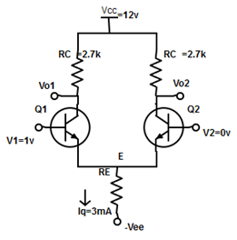
19. From the circuit, determine the output voltage (Assume αF=1)

A. VO1=3.9v , VO2=12v
B. VO1=12v , VO2=3.9v
C. VO1=12v , VO2=0v
D. VO1=3.9v , VO2=-3.9v
20. At what condition does differential amplifier function as a switch
A. 4VT < Vd < -4VT
B. -2VT ≤ Vd ≤ 2VT
C. 0 ≤ Vd < -4VT
D. 0 ≤ Vd ≤ 2VT
21. For Vd > ±4VT, the function of the differential amplifier will be
A. Switch
B. Limiter
C. Automatic gain control
D. Linear Amplifier
22. Change in value of common-mode input signal in differential pair amplifier make
A. Change in voltage across the collector
B. Slight change in collector voltage
C. Collector voltage decreases to zero
D. None of the mentioned
