
During the transition time or turn-on time
Right Answer is:
The forward anode voltage is decreased from 90% to 10% & the anode current increases from 10% to 90% of the initial value
SOLUTION
Turn-ON Characteristics of Thyristor
When the thyristor is forward biased and a positive gate pulse is applied between the gate and cathode, it will be turned ON. But there is a finite transition time to switch from forward OFF-state to forward ON-state for a thyristor. This finite transition time is known as turn-ON time. The turn-ON characteristics of the thyristor are shown in Fig. The turn-ON time tturn-onis the sum of the delay time td, rise time tr and spread time tp and it can be expressed as
tturn-on = td + tr + tp
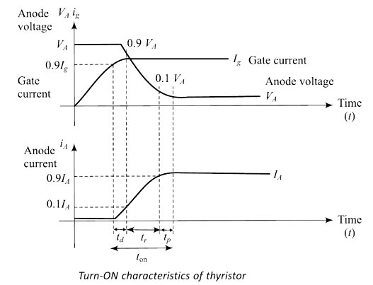
Delay time td:- There is a time delay to turn on a device. The delay time td is the required time interval from the initial anode current, i.e., forward leakage current to reach 10% of the final value of anode current (0.1IA) where IA is the final value of anode current. The delay time td can be measured from the instant of the gate current reaches 0.9Ig to the instant at which anode current reaches to 0.1IA where Ig is the final value of gate current and IA is the final value of anode current. The delay td can also be measured by the time interval during which anode voltage falls from VA to 0.9VA where VA is the initial value of anode to cathode voltage.
This delay time can be decreased by applying high gate currents and high forward anode to cathode voltages. The delay time tat is a fraction of a microsecond.
Rise time tr:– The rise time is the time interval during which the anode current increases from 10% to 90% of the final anode current. During rise time the forward blocking OFF-state voltage decreases, the rise time tr: can be measured from the instant of 90% of forward blocking OFF-state voltage (0.9VA) to the instant at which forward blocking OFF-state voltage reaches to 0.1 VA. The rise time tr: can also be measured from the instant of the gate current reaches 0.9Ig to the instant at which gate current Ig where Ig is the final value of gate current.
The rise time is inversely proportional to the amplitude of the gate current and its build-up rate. The rise time decreases when the high and steep current pulse is applied to the gate of SCR. The value of tr depends on the nature of the anode circuit (R-L and R-C circuits). For example, in a series R-L circuit, the rate of rise of anode current is slow due to the presence of inductance L and rise time is more. In the case of a series R-C circuit, the rate of rise of anode current is high and rise time is less.
During rise time, turn-on losses in the thyristor are the highest due to high anode voltage and large anode current simultaneously occurring in the thyristor. As these losses occur only over a small conducting region, local hot spots may be formed and may be damaged.
Spread time tp:- The spread time is the time interval during which the forward blocking voltage falls from 10% of its value (0.1VA) to the ON-state voltage drop about 1 V to 1.5 V. The spread time can be defined as the time taken by the anode current to rise from 0.9IA to IA. During this time, the conduction spreads over the entire cross-section of the SCR cathode. The spreading time depends on the area of the cathode and the gate structure of SCR.
After spread time, SCR is completely turned on and final steady-state anode current flows through the device and the voltage drop across SCR is about 1 V to 1.5 V. The total turn-ON time of SCR is equal to 1 to 4 µs. The total turn-ON time depends on the anode circuit parameters and the amplitude of the gate current and its wave shape. With the increase of gate current, the turn-ON time will be decreased significantly. The amplitude of the gate current is 3 to 5 times of minimum gate current to trigger thyristor. During the design of the gate triggering circuit, the following conditions should be maintained:
- The gate must be removed just after turn-ON of the thyristor.
- When the thyristor is reverse biased, the gate signal should not be applied.
- The pulse width of the gate pulse must be sufficient so that the anode current must increase to latching current and it must be greater than turn-ON time.