
11. The specification for LM101A op-amp is given as IB =75nA. Determine the value of VIOB– V1.
A. 0.112v
B. 0.750v
C. 0.374v
D. 0.634v
12. The maximum amount by which the two input bias current may differ is known as
A. Input null current
B. Average input bias current
C. Input offset current
D. None of the mentioned
13. A 741 type op-amp has a maximum input offset current of 200nA dc. What conclusion can be derived from this statement?
{ IB1 – Input bias current at inverting input terminal and IB2 – Input bias current at non-inverting input terminal}
A. IB1 may be larger than IB2 by 200nA
B. IB2 may be larger than IB1 by 200nA
C. Iio and IB2 may be equal to 200nA
D. All of the mentioned
14. The maximum magnitude of the output offset voltage is
A. VOIio = RF*Iio
B. VOIio = RF*( IB1+IB2)
C. VOIio = RF*IB1
D. VOIio = RF*( IB1-IB2)
15. Find the output offset voltage of a 741 op-amp; If the gain of the non-inverting amplifier is 8.5 and the feedback resistor = 15kΩ? (IB=200nA for 741 op-amp)
A. 1µv
B. 4 µv
C. 3 µv
D. 2 µv
Gain, A=1+(RF/R1)
=> R1 = RF/(A-1) = 15kΩ/(8.5-1) = 2kΩ.
=> ROM =(R1* RF)/( R1+RF) = 1.76kΩ.
The output offset voltage, VOIB1= VOIB= RF*IB
=> VOIB1= 1.76kΩ*200nA*8.5 = 2.9×10⁻⁶ ≅ 3 µv
[/bg_collapse]
16. Find out the input offset current from the circuit
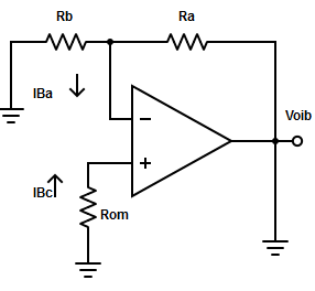
A. Iio = |IBA*IBC|
B. Iio = |IBA+ IBC|
C. Iio = |IBA/ IBC|
D. Iio = |IBA– IBC|
17. Determine the maximum output offset voltage caused by input offset current
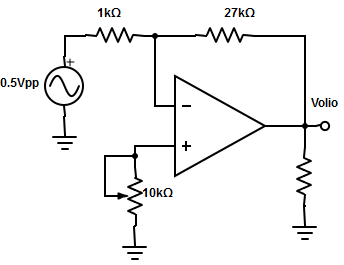
A. 5.4mv
B. 7.3mv
C. 6.9mv
D. 8.1mv
18. Find the total output offset voltage of non-inverting op-amp?
A. VooT = {[1+(RF/R1)]*Vio} + RF*Iio
B. VooT = -[(RF/R1)*Vio] + RF*Iio
C. VooT = -[(RF/R1)*Vio] + Iio
D. None of the mentioned
19. Analyse the circuit and determine the value of total output offset voltage?
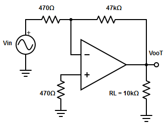
The op-amp is the MC1536 with the following specifications:
Vio = 7.5mv, Iio = 5nA, IB =250nA.
A. 0.12v
B. 1.4v
C. 0.76v
D. 8.5v
Answer:c
The total output offset voltage due to input offset voltage,
VooT = -[(RF/R1)*Vio] + RF*Iio
VooT = [1+(47kΩ/470Ω)]*7.5mv+(47kΩ*50nA.
= 0.7598 ≅ 0.76v.
[/bg_collapse]
20. Which factor affects the input offset voltage, bias current, and input offset current in an op-amp
A. Change in temperature
B. Change in supply voltage
C. Change in time
D. All of the mentioned
21. Thermal voltage drift is defined as
A. △Vio/△T
B. △VF/△T
C. △Iio/△T
D. △IB/△T
22. A completely compensated inverting amplifier is nulled at room temperature 25oC, determine the temperature at which the total output offset voltage will be zero?
A. 50oC
B. 25oC
C. 75oC
D. 125oC