
1. What makes the output voltage equal to zero in practical op-amp?
A. Input offset voltage
B. output offset voltage
C. Offset minimizing voltage
D. Error voltage
2. What happens due to a mismatch between two input terminals in an op-amp?
A. Input offset voltage
B. Output offset voltage
C. Bothe the input and output offset voltage
D. None of the mentioned
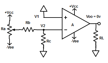
3. Define the polarity of the output offset voltage in a practical op-amp?
A. Positive polarity
B. Negative polarity
C. Positive or negative polarity
D. None of the mentioned
4. The input offset voltage of 741 op-amps has an absolute maximum value of 6mv, which means
A. Minimum difference between input terminals in 741 op-amps can be large as 6mv DC
B. Minimum difference between input terminals in 741 op-amps can be large as 6mv AC
C. Maximum difference between input terminals in 741 op-amps can be large as 6mv DC
D. Maximum difference between input terminals in 741 op-amps can be large as 6mv AC
5. If three different 741 op-amps are taken and the corresponding output offset voltage for each of them is measured. The output voltage in these three op-amps have
A. Same amplitude and polarity
B. Different amplitude and polarity
C. Same amplitude and different polarity
D. Different amplitude and same polarity
6. To reduce the output offset voltage VooT to zero
A. Input offset voltage compensating network is added at the inverting input terminal
B. Input offset voltage compensating network is added at the non-inverting input terminal
C. Input offset voltage compensating network is added at the output terminal
D. None of the mentioned
7. Which of the following op-amp does not need a compensating network?
A. 777
B. 741
C. 748
D. All of the mentioned
8. What will the condition of the op-amp before applying any external input
A. Compensated
B. Biased
C. Balanced
D. Zero
9. Find Thevenin’s equivalent for resistance and voltage?
A. 1-iii, 2-ii, 3-1
B. 1-ii, 2-I, 3-iii
C. 1-I, 2-ii, 3-iii
D. 1-ii, 2-iii, 3-i
10. What is done to compensate for the voltage, when V1 > V2?
A. Move the wiper towards +Vcc
B. Move the wiper towards –Vee
C. Keep the wiper at the center of the potentiometer
D. None of the mentioned
11. Calculate the maximum Thevenin equivalent resistance, if a 10kΩ potentiometer is used?
A. 0.4kΩ
B. 5 kΩ
C. 2.5kΩ
D. 4kΩ
Answer: C
Rmax= Ra/2 || Ra/2 = Ra/4.
Given potentiometer, Ra = 10kΩ
=> Therefore, Rmax = 10kΩ/4 =2.5kΩ.
[/bg_collapse]
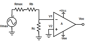
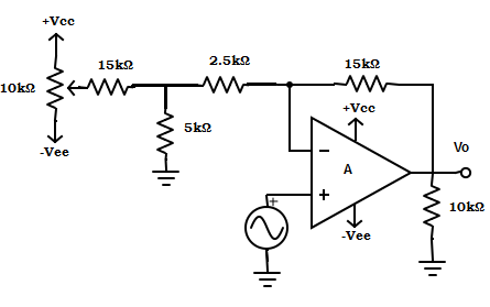
12. Find the input offset voltage for the circuit shown
A. Vio = (Rb*Vmax)/( Rmax+ Rb+ Rc)
B. Vio = Rmax/( Rmax+ Rb+ Rc)
C. Vio = (Rc*Vmax)/( Rmax+ Rb+ Rc)
D. Vio = Vmax/( Rmax+ Rb+ Rc)
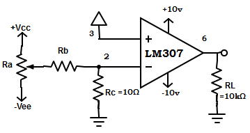
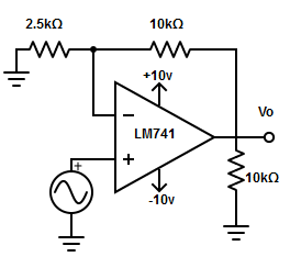
13. Find the value of Ra and Rb from the circuit shown?
A. Ra =4.6kΩ ; Rb= 9kΩ
B. Ra =7.3kΩ ; Rb= 3.4kΩ
C. Ra =2.5kΩ ; Rb= 5.1kΩ
D. Ra =4kΩ ; Rb= 10kΩ
14. Why does an op-amp without feedback is not used in linear circuit application?
A. Due to high current gain
B. Due to high voltage gain
C. Due to high output signal
D. All of the mentioned
15. When the input voltage is reduced to zero in a closed-loop configuration the circuit acts as
A. Inverting amplifier
B. Non-inverting amplifier
C. Inverting and non-inverting amplifier
D. None of the mentioned
16. How the value of output offset voltage is reduced in closed-loop op-amp?
A. By increasing gain
B. By reducing the gain
C. By decreasing bandwidth
D. By reducing bandwidth
17. What happens if R1>>RF in the circuit
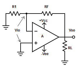
A. Some amount of output offset voltage is present
B. Some amount of input offset voltage is present
C. Some amount of gain voltage is present
D. All of the mentioned
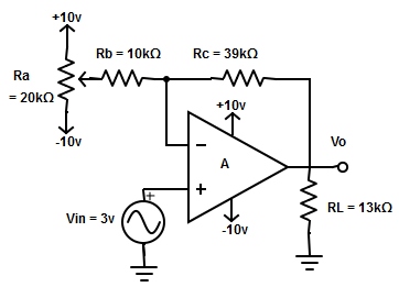
18. Determine the voltage gain for the circuit.
A. 1.1
B. 1.6
C. 1.2
D. 2.2
19. Where does the compensating network connected in an inverting amplifier.
A. Non-inverting input terminal
B. Inverting input terminal
C. Between non-inverting and output terminal
D. Between inverting and output terminal
20. Why closed-loop differential amplifiers are difficult to null?
A. Due to compensating network
B. Due to the feedback loop
C. Due to the input offset voltage
D. None of the mentioned
21. How to achieve maximum CMRR in the given circuit?
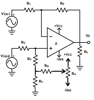
A. R1 = RF
B. RF = R3|| RC+ RB and R1= R2
C. R1= R2 and RF= R3+ RC
D. None of the mentioned
22. What is the advantage of the compensated differential amplifier?
A. All of the mentioned
B. Slightly complex circuit
C. Does not affect CMRR
D. Balanced op-amp
23. The offset voltage in the voltage follower is balanced using
A. Voltage drop across the load resistor
B. Voltage drop across the feedback resistor
C. Compensating network connected to inverting input terminal
D. Compensating network connected to the non-inverting input terminal
24. Find the maximum possible output offset voltage, which is caused by the input offset voltage Vio=15mv?
A. 0.075v
B. 0.75v
C. 0.75v
D. 7.5v
25. Compute the output voltage for voltage follower with offset voltage compensating network?
A. 3.6v
B. 10.8v
C. 26v
D. 33v