Op-Amp Thermal Drift MCQ [Free PDF] – Objective Question Answer for Op-Amp Thermal Drift Quiz

11. When does the op-amp perform better?

A. Low value of SVRR in µV/V
B. High value if SVRR in µV/V
C. Low value of SVRR in dB
D. High value of SVRR in dB

Answer: A

The total value of SVRR in µV/V should be zero. The lower the value of SVRR in µV/V, the better will be the op-amp performance.


12. Write the equation for change in the output offset voltage?

A. △Voo = [-RF/R1)]× [△Vio/△V] ×△V
B. △Voo = [1+(RF/R1)]× [△Vio/△V] ×△V
C. △Voo = [1+(RF/R1)]× [△Vio/△V].
D. None of the mentioned

Answer: B

The change in the input offset voltage is given as

△Voo =[1+(RF/R1)]× [△Vio/△V] × △V

Where

△V = Change in supply voltage +Vcc & -Vee,

△Vio/△V = Supply voltage rejection ratio (µV/V) and

[1+(RF/R1)] = Gain of the differential amplifier.


13. A LM307 amplifier has an SVRR of 92dB, express it in terms of microvolts per volts?

A. 65µV/V
B. 37.98µV/V
C. 25.12µV/V
D. 101.4µV/V

Answer: C

20log(1/SVRR) = 92dB

=> log(1/SVRR) = 92/20

=> 1/SVRR= 104.6

=> SVRR = 1/104.6 = 25.12µV/V.


14. Which value remains the same regardless of whether it is computed from the change in low dc supply or change in +Vcc or -Vee?

A. △V
B. △Vio
C. △Voo
D. None of the mentioned

Answer: D

△V value is the same regardless of whether it is computed from the change in low dc supply or change in +Vcc or -Vee.

For example, suppose that -Vee remains constant at -10v then the +Vcc has to vary from 8 to 12v as a result of a change in low dc voltage. This means that the change in △V in supply voltage +Vcc is 2v in either direction from 10v.


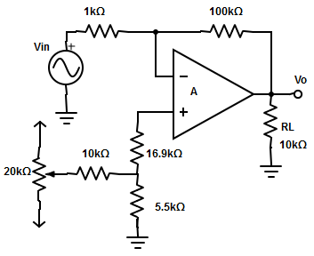
15. Consider LM307 is initially nulled. Suppose, the op-amp has a poor filter, 20mVrms then ac ripple is measured across the terminals. If Vin=0v, determine the change in output offset voltage caused by the change in supply voltage?
drift q7

A. 81µVrms
B. 8.1µVrms
C. 0.81µVrms
D. 810µVrms

Answer: B

The SVRR = 15.85µV/V

for LM307 because of poor filtering and △V= 10mVrms.

The change in output offset voltage

△Voo =[1+(RF/R1)]× [△Vio/△V] ×△V

= [1+(950kΩ/1kΩ)] × (15.85µV/V) × 910mv = 8.1µVrms.


16. What makes the output voltage equal to zero in practical op-amp?

A. Input offset voltage
B. output offset voltage
C. Offset minimizing voltage
D. Error voltage

Answer: A

The input offset voltage is the differential input voltage that exists between two input terminals of an op-amp without any external input and forces the output voltage to zero.


17. What happens due to a mismatch between two input terminals in an op-amp?

A. Input offset voltage
B. Output offset voltage
C. Bothe the input and output offset voltage
D. None of the mentioned

Answer: B

The input offset voltage in op-amp force the output voltage to zero due to the mismatch between two input terminal, there will be voltage produced at the output, and this voltage is called output offset voltage.


18. Define the polarity of the output offset voltage in a practical op-amp?

A. Positive polarity
B. Negative polarity
C. Positive or negative polarity
D. None of the mentioned

Answer: C

The output offset voltage is a DC voltage, it may be positive or negative in polarity depending on whether the potential difference between two input terminals is positive or negative.


19. The input offset voltage of 741 op-amps has an absolute maximum value of 6mv, which means

A. Minimum difference between input terminals in 741 op-amps can be large as 6mv DC
B. Minimum difference between input terminals in 741 op-amps can be large as 6mv AC
C. Maximum difference between input terminals in 741 op-amps can be large as 6mv DC
D. Maximum difference between input terminals in 741 op-amps can be large as 6mv AC

Answer: C

Given that, the absolute maximum value for a 741 is Vio= 6mv. Therefore, the voltage at the non-inverting input terminal may differ from that at the inverting input terminal by as much as 6mv dc. Also, the output offset voltage is a DC voltage and it cannot be an AC voltage.


20. If three different 741 op-amps are taken and the corresponding output offset voltage for each of them is measured. The output voltage in these three op-amps have

A. Same amplitude and polarity
B. Different amplitude and polarity
C. Same amplitude and different polarity
D. Different amplitude and same polarity

Answer: B

Even though the op-amps are of the same type, the output voltage in these three op-amps is not of the same amplitude and polarity, because of mass production.


21. To reduce the output offset voltage VooT to zero

A. Input offset voltage compensating network is added at the inverting input terminal
B. Input offset voltage compensating network is added at the non-inverting input terminal
C. Input offset voltage compensating network is added at the output terminal
D. None of the mentioned

Answer: D

To reduce the VooT to zero, the external circuit is added at the input terminal of the op-amp which will give the flexibility of obtaining input offset voltage of proper amplitude and polarity. The input terminal can be inverting or non-inverting.


22. Which of the following op-amp does not need a compensating network?

A. 777
B. 741
C. 748
D. All of the mentioned

Answer: D

The compensating network is not needed for these op-amps because they have offset null pins.

Scroll to Top