
21. How to achieve maximum CMRR in the given circuit?
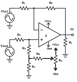
A. R1 = RF
B. RF = R3|| RC+ RB and R1= R2
C. R1= R2 and RF= R3+ RC
D. None of the mentioned
22. What is the advantage of the compensated differential amplifier?
A. All of the mentioned
B. Slightly complex circuit
C. Does not affect CMRR
D. Balanced op-amp
23. The offset voltage in the voltage follower is balanced using
A. Voltage drop across the load resistor
B. Voltage drop across the feedback resistor
C. Compensating network connected to inverting input terminal
D. Compensating network connected to the non-inverting input terminal
24. Find the maximum possible output offset voltage, which is caused by the input offset voltage Vio=15mv?
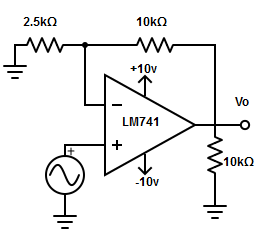
A. 0.075v
B. 0.75v
C. 0.75v
D. 7.5v
25. Compute the output voltage for voltage follower with offset voltage compensating network?
A. 3.6v
B. 10.8v
C. 26v
D. 33v
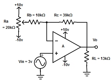
26. Input bias current is defined as
A. Average of two input bias current
B. Summing of two input bias current
C. Difference of two input bias current
D. Product of two input bias current
27. Although the value of input bias current is very small, it causes
A. Output voltage
B. Input offset voltage
C. Output offset voltage
D. All of the mentioned
28. The formula for output offset voltage of an op-amp due to input bias current
A. VOIB= RF*IB
B. VOIB= (RF+R1)/IB
C. VOIB= (1+RF)*IB
D. VOIB= [1+(RF/R1)]*IB
29. Find the input bias current for the circuit given below
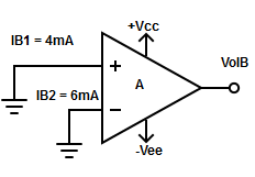
A. 10mA
B. 2mA
C. 5mA
D. None of the mentioned
30. Mention a step to reduce the output offset voltage caused due to input bias current?
A. Use small feedback resistor and resistance at the input terminal
B. Use small feedback resistors
C. Reduce the value of load resistors
D. None of the mentioned