
The P-side emitter in UJT is
Right Answer is:
Heavily doped
SOLUTION
The Unijunction transistor is 2-layer, the 3-terminal solid-state switching device (silicon). It is also called as the double-base diode. The device has a unique characteristic that when it is triggered, its emitter current increases regeneratively (due to negative resistance characteristic) until it is restricted by an emitter power supply. Since the device has one PN junction and three leads it is commonly called UJT.
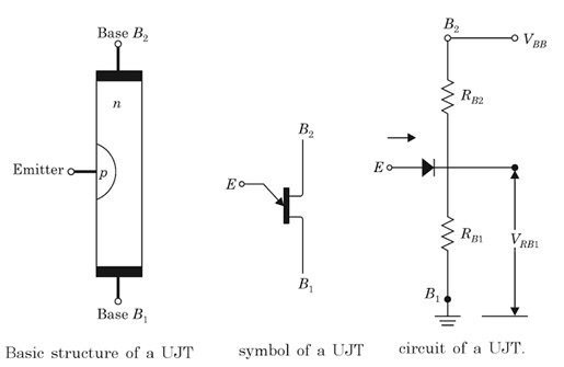
A unijunction transistor (UJT) is a three-terminal semiconductor device having one p-n junction. It is mostly used as a switch and commonly employed in timing circuits, SCR/Triac triggering circuits, oscillators, and so on. It consists of an n-type silicon semiconductor bar having ohmic contacts at each end. The two end connections are called base-1 and base-2, which are labeled as B1 and B2, respectively. This n-type semiconductor is lightly doped. Near terminal B2, a small heavily doped p-region is alloyed which forms a p-n junction with the bar. The terminal to this junction is called emitter (E). The resistance of the silicon bar is called InterBase resistance RBB, i.e. the resistance between the terminals B1 and B2.
Internally UJT acts like a voltage divider consisting of two series resistors RB1 and RB2, while the P-N junction acts like a diode D driving the junction of RB1 and RB2.
Since P-region is heavily doped as compared to N-region, holes are injected from P-region to the lower half of UJT. As N-region is lightly doped the holes injected have a longer lifetime The flooding of the lower half of UJT with holes drastically lowers the resistance RB1. Because of this, the drop across RB1 reduces to a low value, and the emitter current increases.