Ques.91. The schematic symbol for a PN junction diode is
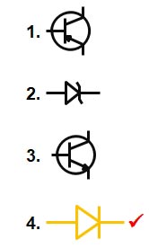
Answer.4. Explanation:- A PN-junction diode can be formed using either germanium or silicon crystal. The PN-junction diode has two terminals, called anode (A) and cathode (K). The P-type region of a PN-junction is called anode and the N-type region is called cathode. The figure represents the circuit symbol of a PN-junction diode. When the diode is forward biased, the current flows from anode to cathode.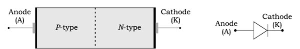
Ques.92. Select the correct statement regarding a semiconductor.
- Acceptor level lies close to the valence band
- N-type semiconductor behave as a conductor at 0°K
- Donor level lies close to the valence band
- All of these
Answer.4. Acceptor level lies close to the valence band Explanation:- Semiconductors can be classified into two types—intrinsic and extrinsic. Intrinsic semiconductors are pure elements like Si and Ge. At 0 K, the valence band is completely filled and the conduction band is empty. Semiconductors obtained by adding impurities (known as doping) to pure semiconductors are called extrinsic semiconductors. Depending on the type of impurity used, semiconductors can be classified into n-type and p-type. If a group V (pentavalent) element like arsenic or phosphorous is added to the group IV element, four electrons of the group V element combine with those of the group IV element to form covalent bonds. The remaining one electron of the impurity atom is very weakly bonded with the parent atom and can easily be excited to the conduction band. This material in which, the conduction is due to these free electrons (called majority charge carriers) is called an n-type semiconductor. The impurity atom which donates free electrons to the crystal is called the donor. The donor energy levels lie below the conduction band edge [Fig.(a)]. If the doping is by group III element, all the three valence electrons enter into covalent bonding, leaving the vacancy of an electron to form saturated bonds. Thus, the doping creates a hole. The material is called a p-type semiconductor with holes as the majority charge carriers. The impurity is called an acceptor impurity. Acceptor levels lie just above the valence band edge [Fig. 12.8(b)]. The Fermi level shifts upwards and lies close to the conduction band in n-type semiconductors. In p-type semiconductors, the Fermi level is closer to the valence band edge. These are also shown in Fig. As the name suggests it is the acceptor band ie it will accept the electrons. Since the electrons present in the valence band. So, the acceptor band being closer to the valence band accepts electrons from it and creates holes. Similarly, in n-type semiconductors, the donor band lies closer to the conduction band as it donates it’s electrons to the conduction band so that the flow of charge carriers can take place easily.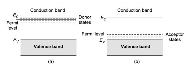
Ques.93. The pair of acceptor impurities for the semiconductor material is
- Gallium and Helium
- Arsenic and Antimony
- Gallium and Indium
- Arsenic and Argon
Answer.3. Gallium and Indium Explanation:- Replacing some Si atoms with atoms from Group III (boron, gallium, indium—also known as acceptor impurities), which have three valence electrons, will create a p-type material. Because four valence electrons are required to form and complete all adjacent electron-pair bonds, a hole is created by the missing bond. A hole can be considered a positive charge which can diffuse or drift through a crystal. This becomes important when an external voltage is applied across the semiconductor, creating an electric field inside the semiconductor which then acts on the holes, causing them to move. The resultant current in p-type material is thus primarily by positive charges, which are also referred to as majority carriers. p-type doping is illustrated in Fig. Important Points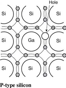
Ques.94. In a P-N junction, the potential barrier is due to the charges on either side of the junction. These charges are
- Majority carriers
- Minority carriers
- Both majority as well as minority carriers
- Fixed donor and acceptor ions
Answer.4. Fixed donor and acceptor ions Explanation:- Let us now consider a p-n junction in which one side a p-type semiconductor and the other side is an n-type semiconductor. The P side has a higher concentration of holes while the n-side has a higher concentration of free electrons. As a result, there is a tendency of the holes in the P-side to diffuse to the N-sides and the electrons in the N side to diffuse to the P-side. Formation of depletion region: The region on both the n- and P sides which are close to the junction develops a low concentration of charge carriers. This happens because, as the electrons on the N-side diffuse towards the p-side, they recombine with the holes close to the junction. The same thing occurs with the hole diffusing from the p-side to the n-side. Since a large number of recombinations occur close to the junction, the charge carrier densities close to the junction decrease drastically. This region close to the junction is called the depletion region or depletion layer. Creation of junction potential: The electric neutrality of the semiconductor material is disturbed the region close to the junction because of the recombination which forms the depletion region. In the p-side of the depletion region, we have an accumulation of fixed negative charge ion since the atoms have acquired electrons from the n-region. Similarly, on the n-type side of the depletion region, there is an accumulation of fixed positive charge ions because the free electrons have moved to p-region. This double layer of positive and negative charges produces an electric field which exerts a force on the electrons and holes against their diffusion. The potential difference corresponding to this electric field is called the potential barrier (or junction potential or barrier potential VB). This name implies that this potential difference acts as a barrier against the diffusion of electrons and holes from their majority side to the minority side. The magnitude of this potential barrier is about 0.3 V in case of germanium and about 0.7 V for silicon-based semiconductor diodes. The width of the depletion layer being of the order of one micron, the electric field that exists in the depletion layer is of the order of 105 Vm-1, which is indeed very high.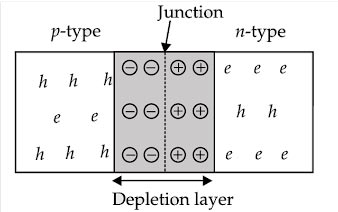
Ques.95. The process of adding, impurities to a semiconductor is known as___
- Polling
- Intrusion
- Plugging
- Doping
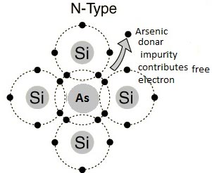
Answer.4. Doping Explanation:- In order to change the properties of intrinsic semiconductors a small amount of some other material is added to it. The process of adding other material to the crystal of intrinsic semiconductors to improve its conductivity is called doping. The impurity added is called dopant. The doped semiconductor material is called extrinsic semiconductor. The doping increases the conductivity of the basic intrinsic semiconductors hence the extrinsic semiconductors are used in practice for the manufacturing of various electronic devices such as diodes, transistors etc. Depending upon the type of impurities, the two types of extrinsic semiconductors are, N-TYPE Impurity The impurity material having five valence electrons is called the pentavalent atom. When this is added to an intrinsic semiconductor, it is called donor doping as each impurity atom donates one free electron to an intrinsic material. Such an impurity is called donor impurity. The examples of such impurity are arsenic, bismuth, phosphorous, Antimony etc. This crests an extrinsic semiconductor with a large number of free electrons, called n-type semiconductor. Germanium and Silicon are tetravalent. The impurity atoms may be either pentavalent or trivalent, i.e., frog group V and III of the periodic table. If a small quantity of a pentavalent impurity (having 5-electrons in tt outermost orbit) like Arsenic (As), Antimony (Sb) or Phosphorus (P) is introduced in Germanium, it replaces the equal number of Germanium atoms without changing the physical state of the crystal. Each of the four out of five valency electrons of impurity says of Arsenic enters into covalent bonds with Germanium, while the fifth valence electron is set free to moo from one atom to the other as shown in Fig. The impurity is called donor impurity as it donates an electron and the crystal called N-type semiconductor. A small amount of Arsenic (impurity) injects billions of free electrons into Germanium thus it creasing its conductivity enormously. In an N-type semiconductor, the majority carriers of charge are the electrons and holes as minority carriers. This is because when donor atoms are added to a semiconductor, the extra free electrons give the semiconductor a greater number of free electrons than it would normally have.
Ques.96. What happens internally on an atomic level when an external electric field is applied to an intrinsic semiconductor?
- More number of electron holes pair combination will be evolved
- More number of electron holes pair combination will be broken
- No electron holes pair combination will be broken
- It will behave as an extrinsic semiconductor
Answer.2. More number of electron holes pair combination will be broken Explanation:- Semiconductors can be classified into two types—intrinsic and extrinsic. Intrinsic semiconductors are pure elements like Si and Ge. At 0 K, the valence band is completely filled and the conduction band is empty. At room temperature, some covalent bonds of an intrinsic semiconductor are broken and liberate some electrons from the orbit and these electrons move freely within the material like gas molecules and are called free electrons. When electrons are liberated from the covalent bonds, then an empty space Is left behind. This empty space (absence of electrons in the covalent bond) is called the hole. Hence an electron-hole pair is generated. These electrons and holes are responsible for conduction of current. In intrinsic semiconductors, the number of electron and holes are equal and very small so its conductivity is very low to be used in different electronic applications. Under the influence of the external electric field, an equilibrium condition is disturbed and electrons move in a direction opposite to that of holes. Holes can be thought of as positively charged particles. The movement of electrons in the conduction band and that of holes in the valance band constitutes current in a semiconductor. Electrons and holes together are known as Charge carders. Thus in a semiconductor, current is constituted by two types of carriers: (a) electrons and (b) holes. In metals, conduction is due to electrons only. It is also possible that some of the free electrons in conduction band may combine with holes in the valence band. This process is known as Recombination. In the process of recombination, an electron loses energy. Intrinsic semiconductor conductivity can be increased either by heating or by adding impurities to them. With the rise in temperature, more and more electron-hole pairs are fanned and more charge carriers are available for conduction. Thus the conductivity of intrinsic semiconductors increases with the increase in temperature (and hence the resistivity decreases with increase in temperature). Increasing conductivity by heating is not a suitable method, therefore we prefer increasing their conductivity by adding impurities to them. These impurities have special characteristics properties and can be taken of trivalent (In, B. Al) or pentavalent (As, Sb, P) elements.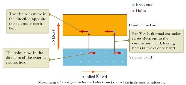
Ques.97. The temperature coefficient of an intrinsic semiconductor is
- Zero
- Positive
- Negative
- Like this of Metal
Answer.3. Negative Explanation:- Properties of intrinsic semiconductors
Ques.98. Hall effect may be used for which of the following?
- Detecting aircraft communication signals
- Determine the carrier concentration
- Determine whether the semiconductor is P or N type
- Calculating the mobility
Answer.3. Determine whether the semiconductor is P or N type Explanation:- A Hall effect sensor is a transducer that produces its output voltage in response to changes in magnetic fields. Applications of Hall effect sensor are
Ques.99. During reverse bias operation of a PN junction, a feeble current flows known as ____________ which is _________ barrier voltage
- Reverse current, Dependent on
- Reverse current, Independent of
- Carrier current, Dependent on
- Carrier current, Independent of
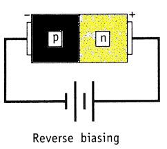
Answer.2. Reverse current, Independent of Explanation:- In the reverse-biased condition, a transient current flows and both the carriers are pulled away from the junction. The increase in barrier energy is given by eV, where V is the voltage applied across the junction. When the potential formed by the widened depletion layer equals the applied voltage, the current ceases except for the small thermal current generated by the minority carriers. This current l is called reverse saturation current, which is independent of the applied reverse voltage (V) and increases with the temperature of the diode. The p-n junction conducts the current easily when forward biased and practically no current flows when it is reverse biased.Reverse biasing
Ques.100. If an atom loses one or more electrons, it becomes ___________.
- Electrically neutral
- Electrically positive
- Electrically negative
- A neutral ion
Answer.2. Electrically positive Explanation:- Atoms are uncharged. The number of protons in an atom is the same as the number of electrons If an atom either gains or loses an electron, it will become electrically charged. When an atom loses or gains electrons, it becomes electrically charged and is called an ion. An ion is an electrically charged atom formed by the loss or gain of one or more electrons. If an atom gains one or more electrons, it becomes a negatively charged ion; an excess negative charge is present because of electrons outnumber protons. If an atom loses one or more electrons, it becomes a positively charged ion; more protons are present than electrons. There is an excess positive charge. Note that the excess positive charge associated with a positive ion is never caused by proton gain but always by electron loss. If the number of protons remains constant and the number of electrons decreases, the result is a net positive charge. The number of protons, which determines the identity of an element, never changes during ion formation. The charge on an ion depends on the number of electrons that are lost or gained. Loss of one, two, or three electrons gives ions with 1+. 2+, or 3+ charges, respectively. A gain of one, two, or three electrons gives ions with 1-, 2-, or 3- charges, respectively.
FOR POWER ELECTRONICS MCQ CLICK HERE
FOR ILLUMINATION MCQ CLICK HERE
FOR MEASUREMENT AND INSTRUMENTATION SYSTEM MCQ CLICK HERE
FOR HEATING AND WELDING MCQ CLICK HERE
FOR TRANSMISSION AND DISTRIBUTION SYSTEM MCQ CLICK HERE
FOR DC MOTOR MCQ CLICK HERE
FOR 3-Φ INDUCTION MOTOR MCQ CLICK HERE
FOR SYNCHRONOUS GENERATOR OR ALTERNATOR MCQ CLICK HERE
FOR Electric Drive MCQ CLICK HERE