Ques.21. The resistivity of an extrinsic semiconductor is about
- 60,000 Ω cm
- 1000 Ω cm
- 2 Ω cm
- 10−6 Ω cm
Answer.3. 2Ω cm Explanation:- The doped semiconductors are called extrinsic semiconductors. At very low temperatures an extrinsic semiconductor has a very low conductivity. The donor levels are filled and there are no electrons in the conduction band, and the acceptor levels are empty leaving no holes in the valence band. As the temperature increases, the donors become ionized and electrons are released into the conduction band, and the acceptor levels become populated leaving holes in the valence band. The electrons in the conduction band and the holes in the valence band cause the extrinsic semiconductor’s conductivity to increase. The figure shows schematically both n-type and p-type semiconductors at absolute zero and at room temperature. At T = 0 in an n-type semiconductor, the donor levels are half filled since each level contains one electron, and the Fermi level is therefore at the energy of the donor impurity level. As the temperature increases to room temperature, the electrons in the donor impurities are released into the conduction band so that the donor levels are depopulated. This implies that the Fermi level has decreased and is below the donor level at room temperature. In the same way, the Fermi level in a p-type semiconductor is at the acceptor level at T = 0 but at room temperature, the Fermi level is above the acceptor level. At room temperature, the resistivity of an extrinsic semiconductor is typically a few ohm-cm while the resistivity of an intrinsic semiconductor is much higher and may depend on the density of unavoidable impurities in the material. Since adding an impurity to semiconductor material increases its conductivity, therefore, the resistivity is very small of about 2Ω cm to 5Ω cm
Ques.22. The impurity level in a semiconductor is about _______ of the pure semiconductor.
- 10 atoms for 108 atoms
- 1 atom for 108 atoms
- 1 atom for 104 atoms
- 1 atom for 100 atoms
Answer.2. 1 atom for 108 atoms Explanation:- Impurity Levels: An intrinsic semiconductor becomes extrinsic semiconductor when a small amount of impurity is added to the given sample. The impurity creates new quantum states in the forbidden energy gap. These quantum states generally appear at a single value of energy and do not spread out into a band for want of interaction between the spare atoms of the impurity material. This value of energy is called impurity level. In an intrinsic semiconductor, this level is absent and enough energy is required to raise an electron from the valence band to the conduction band. An intrinsic semiconductor is capable to conduct a little current even at room temperature. But as it is, it is not useful for the preparation of various electronic devices. The conductivity can, however, be enormously increased by the addition of suitable impurity in a small proportion. It is then called extrinsic (impure) semiconductor. The process by means of which an impurity is added to a semiconductor is known as doping. The amount and type of such impurities have to be closely controlled during the preparation of extrinsic semiconductors. Generally, one impurity atom is added to 108 atoms of a semiconductor. Thus, a semiconductor to which an impurity at a controlled rate is added to make it conductive is known as an extrinsic semiconductor. We know the purpose of adding impurity in the semiconductor crystal is to increase the number of free electrons or holes to make it conductive. If a pentavalent impurity (having 5 valence electrons) is added to a pure semiconductor, a large number of free electrons will exist in it. Whereas, if trivalent impurity (having 3 valence electrons) is added, a large number of holes will exist in the semiconductor.
Ques.23. By adding impurities in semiconductor, the bulk resistance of a semiconductor_______
- Decreases
- Remain the same
- Increases
- None of the above
Answer.1. Decreases Explanation:- Impurity Level in n-type Semiconduction: In an n-type semiconductor the impurity level appears close to the conduction band and therefore, at ordinary temperature electron can easily move from the impurity level to the conduction band and this thing contributes highly towards electrical conductivity. Impurity Level in p-type Semiconductor: In a p-type semiconductor, the impurity level appears close to the valence band. Therefore at ordinary temperature electrons acquire enough energy to move easily from the top of the valence band to the impurity level and leaves positive holes in the valence band which is free to move within the semiconductor and this thing contributes highly toward conductivity. It is clear, therefore, that the addition of donor or acceptor impurity increases the conductivity above the intrinsic level of the semiconductor. In n-type material the majority carriers are electrons and minority carriers are holes while in case of p-type material the situation is reversed.
Ques.24. A hole and electron in close proximity would tend to________
- Repel each other
- Have no effect on each other
- Attract each other
- None of the above
Answer.3. Attract each other Explanation:- An electron excited into the conduction band is a negatively charged particle in a neutral medium which will interact with the resulting hole created in the valence band (positively charged particle). This pair of charged particles is created locally, and they attract each other by the Coulomb force. They form a unit called the exciton. In an exciton, the electron and the hole attract each other and move together as a single particle consisting of a coupled (i.e., not free) electron-hole pair.
Ques.25. In a semiconductor, current conduction is due______
- Only to holes
- Holes and free electrons
- Only to free electrons
- None of the above
Answer.2. Holes and free electrons Explanation:- Current is the movement of charge carriers, such as free electrons, holes, and ions. Electron current is the result of free electrons that are directed to move from one atom to another along a conductive path. Because electrons have a negative charge, they are repelled by areas of negative polarity and are attracted to areas of positive polarity. Electricity was first thought of as the flow of positive charges in a conductor from a point of positive polarity to a point of negative polarity; this is commonly referred to as conventional current. This theory was formulated long before our present understanding of atoms and their subatomic particles. In fact, many of the theories of electricity, including the development of schematic symbols for polarity-sensitive electronic components, are based on the idea of conventional current. The idea is still valid in that conventional current is the flow of positively-charged holes from one atom to another along a conductive path. As an electron jumps from one atom to another, it leaves behind a positively-charged hole. This positively-charged hole attracts another negatively-charged electron. In essence, the two charge carriers switch positions with electrons moving in one direction (from negative to positive) and positively-charged holes moving in the opposite direction (from positive to negative).
Ques.26. The random motion of holes and free electrons due to thermal agitation is called_________
- Ionization
- Pressure
- Diffusion
- None of the above
Answer.3. Diffusion Explanation:- There are two general types of movement of the electrons and holes, diffusion and drifting. Diffusion can be described by the following analogy. Nature does not support the concentration gradient to exist for a long time, i.e. the difference in concentrations of occupying particles between two adjacent regions. Suppose that you have a rectangular tank that is filled with water and has a permeable membrane separating it into two equal parts. On one side of this membrane pour a solution of salt water (sodium chloride) and on the other side pour a solution of potassium chloride. If you let the tank remain unmoved for a few hours and then test the liquid on both sides of the membrane you would find that each of the two solutions is distributed about equally throughout the tank on both sides of the membrane. If you spray some perfume in one corner of your room you immediately feel its effect from other corners because of ‘flow’ due to the concentration gradient. This is applicable for electrons and holes in a semiconductor also. They move from the region of higher concentration to the region of lower concentration. In the same way, the holes and free electrons diffuse throughout a semiconductor. This movement by diffusion is a random movement and is due to the energy of the electrons. The other general type of movement of the electrons in a conductor or semiconductor is by drifting. This movement is caused by some force, e.g., a potential difference between two points in the semiconductor. Drifting is not a random movement like diffusion but is moving in a direction determined by the force causing this movement.
Ques.27. Recombination refers to_______
- Ionization of impurity atom
- Annihilation of holes and electrons
- Breaking of pair-bond
- Thermionic emission
Answer.2. Annihilation of holes and electrons Explanation:- Recombination:- In an intrinsic semiconductor, electrons and holes are produced continuously on account of thermal agitation. Since the electrons and holes move in the crystal in a random manner, there is a possibility of an electron meets a hole. When it happens, both the electron and hole disappear because the electron occupies the position of a hole in a broken covalent bond. The covalent bond is again established. This merging of a free electron and a hole is called recombination. At any temperature, the rate of this recombination is equal to the rate of generation of electrons and holes. However, an electron for a holed travels some distance before it recombines. The average time an electron (or hole) remains free is called its lifetime. At any instant, both types of charge carriers are present in equal numbers at a given temperature.
Ques.28. A forward biased PN junction has a resistance of the____
- Order of Ω
- Order of KΩ
- Order of MΩ
- None of the above
Answer.1. Order of Ω Explanation:- When a manufacturer dopes a crystal so that one half of it is p-type and the other half is n-type, something new occurs. The area between p-type and n-type is called a PN junction. To form the PN junction of a semiconductor, an n-type region of the silicon crystal must be adjacent to or abuts a p-type region in the same crystal. Bias is a potential applied to a PN junction to obtain a desired mode of operation. This potential is used to control the width of the depletion layer. The two types of bias are forward bias and reverse bias. Forward bias is a potential used to reduce the resistance of a PN junction. A forward biased PN junction has a minimum depletion layer width and junction resistance of few ohms. Reverse bias is a potential used to increase the resistance of a PN junction A reverse-biased PN junction has a maximum depletion layer width and junction resistance.
Ques. 29. The battery connections required to forward bias PN junction are
- +ve terminal to p and -ve terminal to n
- -ve terminal to p and +ve terminal to n
- -ve terminal to p and -ve terminal to n
- None of the above
Answer.1. +ve terminal to p and -ve terminal to n Explanation:- When the p-side of a p-n junction is connected to the positive terminal of a battery and n-side is connected to the negative terminal ofthe battery or the applied source, then the p-n junction is said to be forward biased. In the forward biased p-n junction, the holes on p-side are repelled by the positive terminal of the battery and the electrons on the n-side repelled by the negative terminal of the battery. Hence the majority charge carriers move towards the junction. The applied potential opposes the junction potential and hence the resistance or the width of the junction decreases. Once the applied voltage, is greater than the barrier voltage (VB), the majority charge carriers easily diffuse across the junction and the current flows through the diode. When the applied voltage is further increased, the current through the diode increases.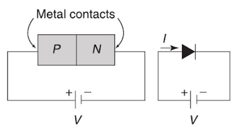
Ques.30. The barrier voltage ar a PN junction for germanium is about_________
- 0.3 V
- 3.5 V
- 3 V
- Zero
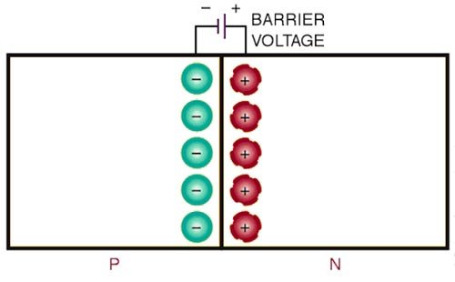
Answer.1. 0.3 V Explanation:- As shown in Fig. the pn junction is the border where the p-type and the n-type regions meet. Each circled plus sign represents a pentavalent atom, and each minus sign is the free electron. Similarly, each circled minus sign is the trivalent atom and each plus sign is the hole. Each piece of a semiconductor is electrically neutrals i.e. the number of Pluses and minuses is equal. The pair of positive and negative ions of the junction is called a dipole. In the dipole, the ions are fixed in the crystal structure and they cannot move around like free electrons and holes. Thus, the region near the Junction is emptied of carriers. This charge-empty region is called the depletion layer also because it is depicted of free electrons and holes. These opposite charges that build up on each side of the junction create a voltage, referred to as the barrier voltage. It can be represented as an external voltage source, even though it exists across the PN junction. The barrier voltage is quite small, measuring only several tenths of a volt. Typically, the barrier voltage is 0.3 V for a germanium PN junction and 0.7 V for a silicon PN junction. This voltage becomes apparent when an external voltage source is applied. A diode requires that the potential barrier voltage of its pn junction must be overcome before it can be forward biased on.