Ques.41. Electron-hole pairs are produced by
- Recombination
- Thermal energy
- Ionization
- Doping
Answer.2. Thermal energy Explanation:- An intrinsic semiconductor is a semiconductor crystal in which electrical conduction arises due to thermally excited electrons and holes. In semiconductors, a single event of covalent bond breaking leads to the generation of two charge carriers, an electron in the conduction band and a hole in the valence band. The process may be represented as Covalent Bond + Thermal Energy ⇒ (Electron + Hole)Pairs As electron and hole are produced simultaneously, the process is called electron-hole pair generation. In the process of generation, a covalent bond is broken and a bound electron is transformed into a free electron. Thermal energy is one of the agents which causes pair generation. Another agent is optical illumination. At any temperature T., the number of electrons generated would be equal to the number of holes produced. If n denotes the concentration of electrons in the conduction band and p is the concentration of holes in the valence band, then n = p After generation, the charge carriers move independently. The electrons move in the conduction band and the holes move in the valence band. Their motion is at random in the respective bands, as long as the external electric field is not applied. It is likely that the electron in conduction band may lose its energy due to collision with other particles in the lattice and fall into the valence band. When a free electron falls into valence band, it merges with a hole. This process is called recombination.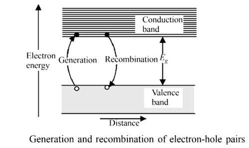
Ques.42. The difference between an insulator and a semiconductor is
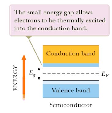
- Wider forbidden gap
- The number of free electrons
- The atomic structure
- All of the above
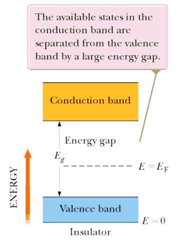
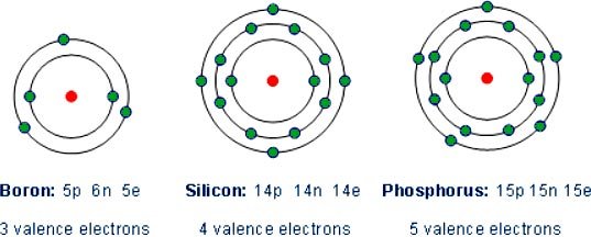
Answer.4. All of the above Explanation:- The main difference between an insulator and semiconductor are Forbidden energy gap The gap between the valence band and the conduction band on the energy level diagram is known as the forbidden band or energy gap. Electrons are never found in this gap. Electrons may jump from back and forth from the bottom valence band to the top conduction band. But they never come to rest in the forbidden band. Insulators In an insulator, the lower band is fined with electrons and the higher band is empty at 0 K. The lower, filled band is called the valence band, and the upper, empty band is the conduction band. (The conduction band is the one that is partially filled in a metal.) It is common to refer to the energy separation between the valence and conduction bands as the energy gap En of the material. The Fermi energy lies somewhere in the energy Band as shown in Figure. In an insulator, the energy gap between valence band and conduction band is very large and approximately equal to 5 eV or more as shown in the figure. Therefore, very high energy is required to push the electrons to the conduction band. For these reasons the electrical conductivity of the insulator is extremely small and may be regarded as nil under ordinary condition (room temperature). The resistivity of insulators lies between 103 to 1017 Ωm at room temperature. At room temperature, the valence electrons of the insulators do not have enough energy to cross over to the conduction band. However, when the temperature is raised some of the valence electrons gain enough energy to cross to the conduction band. Hence, the resistance of the insulator decreases with an increase of temperature, i.e., an insulator has a negative temperature coefficient of resistance. Semiconductor:- Semiconductors have the same type of band structure as an insulator; but the energy gap is much smaller, on the order of 1 eV. At low temperature, the valence band of a semiconductor is completely filled and the conduction band is completely empty as shown in figure 9. 3b. Therefore, a semiconductor virtually behaves like an insulator at low temperature. However, at room temperature, some electrons cross over to the conduction band giving a little conductivity to the semiconductor. As the temperature is increased more valence electrons cross over to the conduction band and conductivity increases. This shows that electrical conductivity of a semiconductor increases with the increase of temperature, i.e., a semiconductor has a negative temperature coefficient of resistance. The forbidden energy gap for germanium is 0. 7 eV and for silicon 1.1 eV Atomic Structure To understand how semiconductors work it is necessary to study briefly the structure of matter. All atoms are made of electrons, protons, and neutrons. Most solid materials are classed, from the standpoint of electrical conductivity, as conductors, semiconductors or insulators. To be the conductor, the substance must contain some mobile electrons—one that can move freely between the atoms. These free electrons come only Tom the valence (outer) orbit of the atom. Physical force associated with the valence electrons binds adjacent atoms together. The inner electrons below the valence level do not normally enter into the conduction Process. Conductivity depends on the number of electrons in the valence orbit. Electron diagrams for three typical elements, Boron, silicon, and phosphorous are shown in Figs. 1, 2, 3. These elements can all be used in semiconductor manufacture. The degree of conductivity is determined as follows: 1. Atoms with fewer than four valence electrons are good conductors. 2. Atoms with more titian four valence electrons are poor conductors. 3. Atoms with four valence electrons are semiconductors. Fig. 1 shows Boron which has three valence electrons. When there are less than four valence electrons they are loosely held so that at least one electron per atom is nominally free; hence aluminum is a good conductor. This availability of free electrons is also true of copper and most other metals. Silicon (Fig. 2) has four valence electrons. This makes it neither a good conductor nor good insulator, hence its name Semiconductors. Silicon also has four valence electrons and is a semiconductor. Fig. 3 shows Phosphorus with five valence electrons. When there are more than four valence electrons, they are lightly held in orbit so that normally none are free. Hence phosphorus and similar elements are poor conductors (insulators). Number of free electrons Electrons in the valence shell can gain energy. If these electrons gain enough energy from an external force, they can leave the atom and become free electrons, moving randomly from atom to atom. Materials that contain a large number of free electrons are called conductors. Insulator, the opposite of conductors, prevent the flow of electricity. Insulators are stabilized by absorbing valence electrons from other atoms to fill their valence shells, thus eliminating free electrons. Mica is the best insulator because it has the fewest free electrons in the valence shell. A perfect insulator will have atoms with a full valence shell. This means it cannot gain electrons. Halfway between conductors and insulators are a semiconductor. Semiconductors are neither good conductors nor good insulators but are important because they can be altered to function as conductor and insulator.
Ques.43. Holes in N-type Semiconductor are
- Minority carriers produced by thermal energy
- Minority carrier produced by doping
- Majority carrier that is thermally produced
- Majority carriers that are produced by doping
Answer.1. Minority carrier produced by thermal energy Explanation:- The process of adding either a pentavalent element or a trivalent element to a pure semiconductor is called doping. The doped semiconductor is called extrinsic semiconductor. The doping material that is added to a pure semiconductor is also referred to as impurity material. Depending upon whether a pentavalent or trivalent doping material is added, extrinsic semiconductors are respectively called n-type semiconductor or p-type semiconductors. The number of charge carriers, either an excess of electrons or deficiency of electrons (causing holes in a material), can be altered by doping or adding very small quantities of impurities to a semiconductor material. A doped semiconductor always has an excess of one type of charge carrier. For example, excess electrons make it an N-type semiconductor “N” stands for negative. Excess holes make it a P-type semiconductor.”P” stands for positive. Each of these materials responds to positive or negative current flow oppositely. N-Type Semiconductor The n-type semiconductor is formed by doping a pure silicon or germanium crystal with a material having five valence electrons. Antimony, arsenic, and phosphorous are pentavalent materials as can be read from the periodic table. If arsenic in very small quantity is added to a silicon crystal, four out of five valence electrons will form covalent bonds with silicon atoms with one electron left free. Thus, for each arsenic atom, there will be one free electron. Although the percentage of arsenic added is very small, the number of atoms being very large, a huge amount of free electrons will be available in the n-type semiconductor. These electrons being free (not taking part in any covalent bonding) are loosely bound to their parent atom and are free to conduct electricity. Fig. shows impurity atoms of arsenic having five valence electrons forming covalent bonds with germanium having four valence electrons. There is one extra electron for each impurity atom added. This extra electron is not a part of any covalent bond and is called a free electron. It is important to understand that in N-type semiconductors, although electrons (negative charges) are the majority carriers, but the semiconductor doped with impurity remains electrically neutral. Free electrons and holes are generated in pairs due to thermal energy and negative charge of electrons donated by impurity atoms is exactly balanced by the positive charge of the immobile ions. Hence in n-type material, the electrons become the majority carriers and the holes generated by thermal energy constitute minority carriers.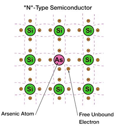
Ques.44. The depletion region is created by
- Ionization
- Diffusion
- Recombination
- All of the above
Answer.2,3. Diffusion, Recombination Explanation:- As soon as a PN junction is formed, electrons frog n-type material diffuse into p-type material and fill some of the holes there. At the same time, holes from p-type material diffuse into the n-type material and are filled by electrons This migration of charge carriers (free electrons and holes result in n-section acquiring a positive charge and a p-section a negative charge. These two layers of positive and negative charges form depletion region or depletion layer. Within a very short time, the steady-state conditions are reached and further movement of charge carriers (free electrons and holes) across the junction stop. It is because the electric field set up by the depletion layer acts as a barrier to further diffusion of electrons into the p-region and holes into the n-region. The depletion layer is so called because, in this region, the charge carriers (free electrons and holes) have been depleted (i.e. emptied). The small region on both sides of the PN junctions sluice is depleted of charge carriers (free electrons and holes) and has only immobile ions is called depletion layer When the junction is formed, the following processes are initiated: Ionization:- Ionization is the process of removing orbital electrons from atoms to produce positive ions and free electrons. In semiconductors and insulators, ionization always produces electron-hole pairs where an electron is removed and a mobile hole is generated in the valence band. Both photons (gamma rays) and charged particles (electrons, protons, and heavy ions) cause ionization. The number of electron-hole pairs generated depends on the material’s band gap and the quantity of energy absorbed by the ionized electron. About 3.6 eV is needed to create an electron-hole pair in silicon. In semiconductor devices, the main effects of ionization are positive charge buildup in the insulator. In positive charge buildup, some of the electrons from the electron-hole pairs leave the insulator so that the trapped holes produce positive charge in the insulator. The localized electrons at the insulator-semiconductor interface can generate interface energy states distributed throughout the band gap. Photocurrents are caused by electron-hole pairs generated in the junction’s depletion region and by minority carriers within a diffusion length of the depletion region. The depletion region is a region void of any charges. So obviously ionization is ruled out because ionization creates charges. Diffusion is a process where charges move from higher concentration to lower concentration with or without the influence of field. They are responsible for charge movement through the junction. Finally, recombination is a process where the electrons and holes neutralize charged atoms. So, diffusion results in recombination which creates a depletion region.
Ques.45. The depletion region consists of
- Nothing but minority carriers
- Positive and negative ions
- No majority carrier
- (ii) and (iii)
Answer.4. (ii) and (iii) Explanation:-
Ques.46. The terms BIAS means
- Ratio of majority to minority carriers
- Amount of current across PN junction
- D.C voltage applied to an electronic device
- None of the above
Answer.3. D.C voltage applied to an electronic device Explanation:- Applying external d.c. voltage to an electronic device is called biasing. Depending upon the polarity of the d.c. voltage externally applied to it, Be biasing is classified as forward biasing and Reverse biasing. Forward Biasing of P-N Junction Diode If an external d.c. voltage is connected in such a way that the p-region terminal is connected to the positive of the D.C voltage and the n-region is connected to the negative of the d.c. voltage, the biasing condition is called forward biasing. The p-n junction is said to be forward biased. Reverse Biasing of P-N Junction Diode If an external d.c. voltage is connected in such a way that the p-region terminal of a p-n junction is connected to the negative of the battery and the n-region terminal of a p-n junction is connected to the positive terminal of the battery, the biasing condition is called reverse biasing of a PN junction.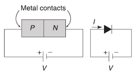
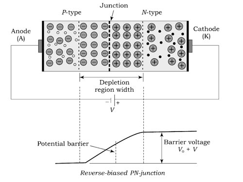
Ques.47. When a voltmeter is connected across a forward-biased diode it will read a voltage approximately equal to
- Bias battery voltage
- 0 V
- Diode barrier potential
- None of the above
Answer.3. Diode barrier potential Explanation:- Barrier potential. Once PN junction is formed and depletion layer created, further movement of charge carriers across the junction stops i.e. depletion layer acts as a barrier to the movement of charge carriers across the junction. There exists a potential difference across the depletion layer and is called barrier potential. The barrier potential of a PN junction depends upon several factors including the type of semiconductor material, the amount of doping and temperature. The typical barrier potential is approximate: For silicon VO= 0.7 V; For germanium, VO = 0.3 V Forward biased A diode is best tested by measuring the voltage drop across the diode when it is forward-biased. A forward-biased diode acts as a closed switch, permitting current to flow. A diode is forward-biased when the positive test lead is on the anode and the negative test lead is on the cathode. If the diode is germanium, the meter should display from 0.2 to 0.3 (volt) for a good diode; if the diode is silicon, the meter should display between 0.6 and 0.7 (volt) for a good diode. (Actually, some may read slightly less or more.) This is called the forward bias Condition—the positive lead of the meter to positive (anode) end of the diode and negative lead of the meter to the negative (cathode) end. Forward bias (positive to positive and negative to negative) breaks down the barrier or depletion region in a diode, and current flows through the diode. Bias is just another name for a DC voltage. Hence in forwarding bias condition, the diode read voltage approximately equal to barrier potential voltage. Reversed Biased A diode is reverse-biased when the positive test lead is on the cathode and the negative (black) test lead is on the anode. If the diode is germanium or silicon, the meter should display infinite, which may be represented by the infinity symbol (so) or “OL” (overload) for a good diode This is called the reverse-biased Condition—positive lead of meter to negative (cathode) end of diode and negative lead of meter to positive (anode) end. Reverse bias enlarges the depletion region (the “no electron zone”) in a diode, and no current flows through the diode. Note:- Consequently, a germanium diode must read about 0.2 to 0.3 (volt) in the forward bias condition and infinite in the reverse bias condition to be “good.” If a germanium diode reads 0.2 to 0.3 in both the forward and reverse bias conditions, it is bad (shorted) and must be replaced. Also, if a germanium diode reads infinite in both the forward and reverse bias conditions, it is bad (open) and must be replaced. The same holds true for a silicon diode. A silicon diode must read about 0.6 to 0.7 (volt) in the forward bias condition and infinite in the reverse bias condition to be good. If a silicon diode reads 0.6 to 0.7 in both forward and reverse bias, it is bad (shorted) and must be replaced. Also, if a silicon diode reads infinite in both the forward and reverse bias conditions, it is bad (open) and must be replaced. Testing of diode
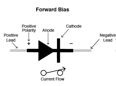
Ques.48. When the positive lead of a multimeter is connected to the anode of a diode and the negative lead to the cathode the diode is
- Reverse biased
- Open
- Forward biased
- None of the above
Answer.3. Forward Biased
Explanation:-
A diode is forward-biased when the positive test lead is on the anode and the negative test lead is on the cathode. If the diode is germanium, the meter should display from 0.2 to 0.3 (volt) for a good diode; if the diode is silicon, the meter should display between 0.6 and 0.7 (volt) for a good diode. (Actually, some may read slightly less or more.) This is called the forward bias Condition—the positive lead of the meter to positive (anode) end of the diode and negative lead of the meter to the negative (cathode) end.
Ques.49. When the voltage is applied to semiconductor holes will flow
- Away from the negative terminal
- Toward negative terminal
- In the external circuit
- None of the above
Answer.2. Toward negative terminal Explanation:- Forward bias is obtained with the negative terminal of the battery connected to the N-side and positive terminal connected to the p-side. Since the hole is a positive charge carrier and an electron is a negative charge carrier hence the negative terminal will repel free electrons in the n-section towards the junction, and the positive terminal on the p-side will push the holes towards the negative terminal junction. These free electrons and holes will then combine at the junction.
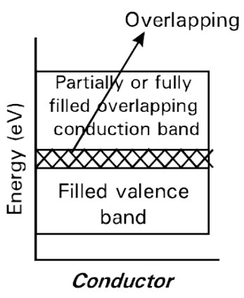
Ques.50. At room temperature, a conductor has how many holes?
- Many
- None
- Only those produced by thermal energy
- Same number as free electrons
Answer.2. None Explanation:- Conductors Conductors are characterized by high electrical conductivity. These are the solids in which plenty of free electrons are available for electrical conduction. Example silver, copper, iron, aluminum etc. In general, the resistivity of conductors lies in the range of 10-9 Ωm at room temperature. In a conductor the conduction band and the valence band overlap each other as shown in the figure so that the electrons can readily pass into the conduction band, i.e., the electrons can readily move under the influence of applied field. For conductors, the energy gap is of the order of 0.01 eV. In metal, there is just a conduction band that is filled to some level with electrons, allowing current to flow freely. Some of the electrons may be thermally excited and thus leave some lower energy level unoccupied, but that doesn’t really contribute to the conductivity properties. “Holes”, i.e. the absence of an electron in an available energy level of the valence band, are only important in semiconductors. Holes are introduced, because (typically) in semiconductors we have two energy ranges in which the presence of electrons is allowed, which are significantly separated. Moreover Fermi level on the typical case is between these allowed energy ranges (between valence and conduction bands).