Ques.61. The most widely used semiconductor in electronics device is
- Germanium
- Carbon
- Copper
- Silicon
Answer.4. Silicon Explanation:- Silicon is the most widely used semiconductor material because it has a useful temperature range and is abundant, cheap, and easy to manufacture. Germanium was among the first semiconductor materials to be developed and is less widely used than silicon, but it is useful in very high-speed devices when alloyed with silicon. High-speed semiconductors widely use gallium-arsenide. It is the most commonly used material after silicon; however, it is more expensive and more difficult to manufacture. Silicon carbide has been used to create blue light-emitting diodes (LEDs), and it can withstand high operating temperatures.
Ques.62. The energy gap between valence band and conduction band in insulators is
- 5 eV
- 1 eV
- 2 eV
- 3.5 eV
Answer.1. 5 eV Explanation:- Forbidden energy gap The gap between the valence band and the conduction band on the energy level diagram is known as the forbidden band or energy gap. Electrons are never found in this gap. Electrons may jump from back and forth from the bottom valence band to the top conduction band. But they never come to rest in the forbidden band. Insulators In an insulator, the valance band is completely filled and there is a large forbidden gap Eg between the valence band and the conduction band. The gap is generally between 5eV to 10 eV. Under an applied electric field the valence electrons cannot gain enough energy to jump to the conduction band. Further, the exclusion principle does not permit any transition within the valence band. Therefore, no current can flow. Note that the forbidden gap is so large that the electrons cannot go from the valence band to the conduction band by thermal excitation. At room temperature, the thermal energy kT is negligible as compared to the forbidden gap. The resistivity of insulators lies between 103 to 1017 Ωm at room temperature. However, when the temperature is raised some of the valence electrons gain enough energy to cross to the conduction band. Hence, the resistance of the insulator decreases with an increase of temperature, i.e., an insulator has a negative temperature coefficient of resistance.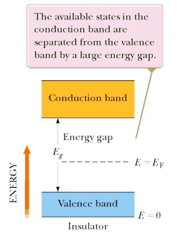
Ques.63. The energy band in which free electrons exist is
- First band
- Second band
- Conduction band
- Valence band
Answer.3. Conduction band Explanation:- A large number of discrete but closely spaced energy levels is called an energy band. Out of all the energy bands, Three bands are most important to understand the behavior of solids. These bands are, Valence Band:- A series of energy Levels having valance electrons form a band called valance band”. In other words, the valance is defined by a band which is occupied by the valance electrons or a band having the highest occupied band energy. The valance band may be partially or completely filled up depending on the nature of the crystal. The valence electrons form the covalent bonds and are not free. But when certain energy is imparted to them, they become free. Conduction Band: The next higher permitted band is the conduction band. The electrons occupying this band are called conduction electrons and the band is called conduction band. This band can also be defined as the lowest unfilled energy band. This band may be empty or partially filled. In this band, electrons move freely. Under normal condition, the conduction band is empty and once energy is imparted, the valence electrons jump from valence band to conduction band and become free. While jumping from valence band to conduction band, the electrons have to cross an energy gap. Forbidden Gap: The energy gap which is present separating the conduction band and the valence band is called forbidden band or forbidden gap.T his band is formed by series of energy levels above the top of the valence band and below the bottom of the conduction band. It should be noted that no, a free electron can exist in this band. When enough energy is given to an electron in the valence band, it jumps the forbidden band and enters the conduction band. When an electron jumps to the conduction band by absorbing energy, a covalent bond is broken and a positively charged hole is created. This hole is filled up by another electron from the adjacent atom. This process is repeated as if a hole moves from one to another place.
Ques.64. The energy gap between valence band and conduction band in conductors is
- 5 eV
- Zero
- 10 eV
- 15 eV
Answer.2. Zero Explanation:- Conductors:- In the case of conductors, no forbidden band is there and the valence and conduction bands overlap each other. Here a large number of free electrons are available for electric conduction, and electrons from valence band freely enter into the conduction band. Now since in the case of conductors, there is no forbidden band, so holes are not created at all and the total flow of current is due to the motion of electrons only.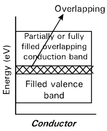
Ques.65. The majority carriers in a semiconductor are produced by
- Doping
- Electron-holes pairs
- Bound electrons
- None of the above
Answer.1. Doping Explanation:- A pure silicon crystal or germanium crystal is known as an intrinsic semiconductor. For most application, there are not enough free electrons and holes in an intrinsic semiconductor to produce a usable current. The electrical action of these can be modified by doping means adding impurity atoms to a crystal to increase either the number of free holes or number of free electrons. When a crystal has been doped, it is called an extrinsic semiconductor. They are of two types n-type semiconductor having free electrons as majority carriers, p-type semiconductor having free holes as majority carriers. By themselves, these doped materials are of little use. However, if a junction is made by joining p-type semiconductor to n-type semiconductor a device is produced which is extremely used known as a diode. It will allow current to How through it only in one direction. The unidirectional properties of a diode allow current flow when forward biased and disallow current flow when reversed biased. This is called rectification process and therefore it is called rectifier.
Ques.66. The minority carrier in a semiconductor is produced by
- Doping
- Electron-hole pairs
- Bound electrons
- None of the above
Answer.2. Electron-hole pair Explanation:- The majority carriers in an n-type semiconductor are free electrons acquired by the doping process and the minority carriers are holes produced by thermally generated electron-hole pairs. The majority carriers in a p-type semiconductor are holes acquired by Ike doping process. and the minority carrier is free electrons produced by the thermally generated electron-hole pair. These electron-hole pairs are thermally produced because the electron has acquired enough energy from external heat to break away from its atom. A free electron will eventually lose energy and fall back into a hole. This is called recombination. Electron-hole pairs are continuously being thermally generated so there are always free electrons in the material. The minority carriers are thermally produced and they exist only for short time after which they recombine and neutralize each other. In the meantime, other minority carriers have been produced and this process goes on and on. The number of these electron-hole pairs that exist at any one time depends upon the temperature. The number of majority carriers is, however, fixed depending on the number of impurity atoms available. But it is to be noted that the minority carrier concentration in the doped semiconductors is smaller than that of intrinsic one because the presence of excess majority carriers in extrinsic semiconductors ‘kills’ some of the minority carriers by recombination process.
Ques.67. The process of adding an impurity to an intrinsic semiconductor is called
- Recombination
- Ionization
- Atomic modification
- Doping
Answer.4. Doping Explanation:- It is possible to effectively increase the electrical conductivity of germanium or silicon by introducing some impurity in the process of crystallization. Such semiconductors are called extrinsic semiconductors. The addition of the foreign impurity to an intrinsic semiconductor in controlled quantities to promote conductivity is termed as Doping. A doped intrinsic semiconductor is called an extrinsic semiconductor.
Ques.68. In an intrinsic semiconductor
- There are no free electrons
- There are only holes
- Free electrons are thermally produced
- Cannot say
Answer.3. Free electrons are thermally produced Explanation:- A pure semiconductor in which holes and electrons arc created solely by thermal excitation across the energy gap is called an intrinsic semiconductor; the holes and electrons thus created are known as intrinsic charge carriers and the conductivity is termed as intrinsic conductivity. In an intrinsic semiconductor, the concentration of holes in the valence band and that of electrons in the conduction band is always the same at all temperatures, since the thermal excitation of an electron to the conduction band by breaking a covalent bond in the valence band creates one and only one hole. At room temperature (T> 0 K), the valence electron acquires a sufficient amount of thermal energy. As a result, breakage of covalent bonds takes place releasing free electrons. These free electrons create a vacancy in its initial position in the crystal. This vacancy is known as a hole and is assumed to carry a positive charge equivalent to the charge of the electron. These free electrons, due to acquiring of sufficient thermal energy, cross the energy gap and enter into the conduction band from the valence band and occupy the energy levels in the conduction band. The electrons leaving the valence band create holes in its place. Thus, the valence band has holes while the conduction band has electrons. The corresponding crystal structure along with the energy band structure is as shown in Fig. In the intrinsic semiconductor, the electrons and holes are generated in pairs and at any given temperature the volume concentration of electrons is equal to that of holes. With the rise in temperature, more and more electron-hole pairs are formed and more charge carriers are available for conduction. Thus the conductivity of intrinsic semiconductors increases with the increase in temperature (and hence the resistivity decreases with increase in temperature).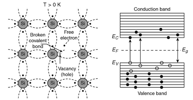
Ques.69. When a PN junction is forward biased, the current in the external wires is
- Zero
- By free electrons
- By Holes
- By both free electrons and holes
Answer.2. By free electrons Explanation:- In a forward biased PN-junction, an external voltage source (battery) is connected to the PN junction in such a way that the positive terminal of the voltage source is connected to the P-type region and the negative terminal of the voltage source is connected to the N-type region. Whenever a PN junction is forward biased, the holes are repelled by the positive terminal of the voltage source. Then holes are forcefully moved towards the junction. Correspondingly, the electrons are repelled by the negative terminal of the voltage source and these electrons are also forcefully moved towards the junction. As carriers (holes and electrons) get energy from the external voltage source, some of the holes and electrons are able to enter into the depletion layer and recombination takes place. Consequently, the width of the depletion layer decreases as well as the potential barriers (Via) at depletion region is decreased. Therefore, more majority carriers diffuse across the junction and a large amount of current will flow through the PN junction. An ideal PN junction has a voltage drop across the crystal. When recombination between free electrons and holes occurs, an electron from the negative terminal of the external voltage source enters into the N-type region and moves towards the junction. In the P-type region, an electron breaks a covalent bond in the crystal and enters into the positive terminal of the external voltage source. In this way, for each electron, one covalent bond in the crystal breaks, generating a hole which then drifts towards the junction. The current in the p-region is due to the movement of holes which are majority carrier. This is the hole current. While the current in the n-region is due to the movement of free electrons which are majority carriers. This is the electron current. Hence the overall forward current is due to me majority charge carrier. These majority carriers can then travel around the closed circuit and a relatively large current flows. The direction of flow of electrons is from negative to positive of the battery. While the direction of the conventional current is from positive to negative of the battery as shown. Therefore, the current flowing through the PN junction is the sum of electron diffusion current in the N-type region and hole diffusion current in the P-type region. Though the total current inside the semiconductor is due to free electrons and holes, the current in the external wire is fully by electrons. When the voltage source is continuously present in the circuit, the current flows continuously in the external circuit. If the applied voltage is increased, the current increases and it is in the order of several milliamperes (mA). Actually, the amplitude of the current depends on the resistance of the semiconductor material. Conventional Current Flow versus Electron Current Flow Before electrons were known, Benjamin Franklin surmised that current was a flow of positive charges moving from positive to negative in a circuit. Franklin’s belief became so accepted that even after electrons were discovered and scientists learned that current flow consists of electrons moving from negative to positive, the old idea was hard to give up. As a result, the “idea” of positive charges moving from positive to negative is still often used. It is referred to as conventional current flow or less formally as hole flow. The conventional current flow theory has gotten a boost in recent years because it helps explain how semiconductors work: Positively charged holes move from positive charges to negative charges as electrons move from negative charges to positive charges.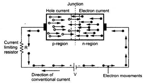
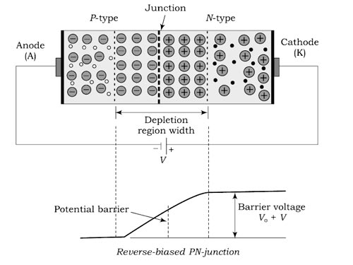
Ques.70. When a PN Junction is reversed biased, the current is due to
- Zero
- By minority carrier
- By both free electrons and holes
- By free electrons
Answer.2. By minority carrier Explanation:- Reverse-Biased PN-Junction When a voltage source (battery) is connected to a PN-junction in such a way that negative terminal of the voltage source is connected to the P-region and the positive terminal of the voltage source is connected to the N-region, the PN junction is called reverse-biased PN junction. When a PN junction is reverse biased, in the P-region the holes are attracted towards the negative terminal of the supply voltage. Similarly, the electrons are attracted to the positive terminal of the supply voltage in the N-region. Hence, the majority of carriers are drawn away from the junction. As the barrier potential is increased, it is very difficult for the majority carriers (holes in the P-type region and electrons in the N-type region) to diffuse across the junction. Consequently, there is no current due to majority carriers in a reverse-biased PN junction. Hence, the reverse biased PN junction provides a very high resistance. However, minority carriers (electrons in the P-type region and holes in the N-type region) drift across the junction and the barrier potential helps the minority carriers to cross the junction. In a reverse-biased PN junction, whenever the minority carriers are generated throughout the crystal due to thermal energy, these minority carriers are drifted across the junction. As a result, a very small amount of current flows through the reverse biased PN junction. This current depends on the number of minority carriers which are diffused across the junction. So, the amplitude of the current depends on the generation of minority carriers within the P-type region and N-type region. Usually, the generation of minority carriers depends on the temperature and it is independent of the applied reverse-bias voltage. Hence, the current flow due to minority carriers remains constant and it cannot be changed with increasing or decreasing the applied voltage. This current is called reverse saturation current.