Ques.41. The average power in a pure inductive circuit is ______ (SSC 2016, Set-1)
Zero
Maximum
VI
V.I.Cosφ
Answer.1. Zero
Explanation:-
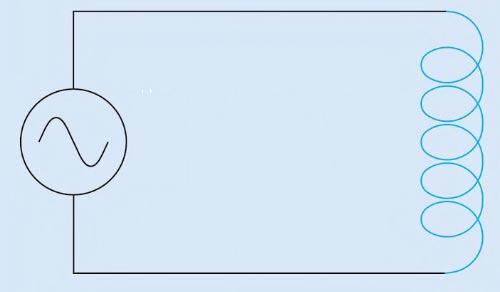
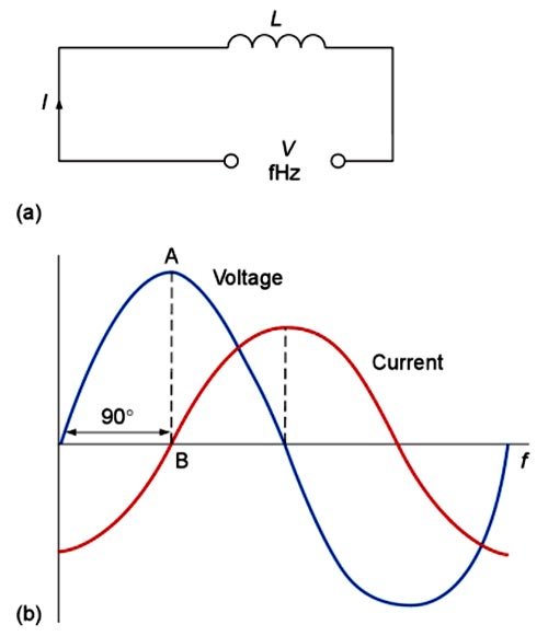
Pure Inductive circuit
Consider a purely inductive circuit as shown in the figure.
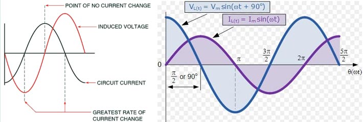
In a purely inductive circuit, the current lags the voltage by 90°. To understand this we must have to consider the relationship between the applied voltage and the induced voltage. How the current and applied voltage can become 90° out of phase with each other can best be explained by comparing the relationship between the current and induced voltage. As we know that the induced voltage is proportional to the rate of change of the current (speed of cutting action). At the beginning of the waveform, the current is shown at its maximum value in the negative direction. At this time, the current is not changing, so the induced voltage is zero. As the current begins to decrease in value, the magnetic field produced by the flow of current decreases or collapses and begins to induce a voltage into the coil as it cuts through the conductors (Figure.).
The greatest rate of current change occurs when the current passes from negative, through zero and begins to increase in a positive direction. Because the current is changing at the greatest rate, the induced voltage is maximum. As current approaches its peak value in the positive direction, the rate of change decreases, causing a decrease in the induced voltage. The induced voltage will again be zero when the current reaches its peak value and the magnetic field stops expanding. It can be seen that the current flowing through the inductor is leading the induced voltage by 90°. Because the induced voltage is 180° out of phase with the applied voltage, the current lags the applied voltage by 90°.
Or Mathematically we can prove the same
Consider the sinusoidal current and voltage waveform. As we know that the voltage leads the current by 90°. i.e
I = Imsinωt V = Vmsin(ωt + 90°)
The value of current will be maximum when ωt = 90°
Then I = Imsin90° I = Im
V = Vmsin(180°)
V = 0
Hence when the current will reach its maximum value the voltage will become zero.
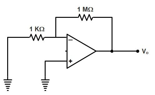
Ques.42. An OP-AMP has an offset voltage of 1 mV and is ideal in all other respects. If this OP AMP is used in the circuit shown in the figure, the output voltage will be approximately (SSC 2016, Set-1)
2.5 V
3.4 V
1 V
Zero
Answer.3. 1V
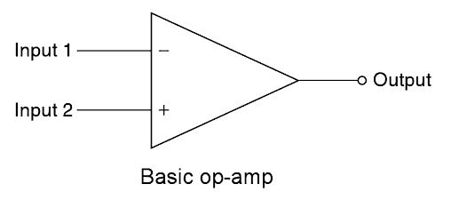
The op-amp is known as the differential amplifier because it amplifies the voltage difference of the inverting and non-inverting terminals. A third terminal represents the operational amplifiers output port which can both sink and source either a voltage or a current.
PROPERTIES OF THE IDEAL OPERATIONAL AMPLIFIER
An ideal op-amp should have the following properties:
Gain must be infinite
Output voltage must be zero when input voltages are the same or when both are zero
The input resistance must be infinite
The output resistance must be zero
The common-mode rejection ratio (CMMR) must be infinite
Now coming back to the Question
Input offset voltage(vio )the voltage that must be applied between input terminals of OPAMP to ensure zero output for zero input.
vio = |v+ – v–|
As non-inverting terminal of the given op-amp is connected to the ground.
V+ = 0 Vio = |0 – v–| = v– V – = R1 /(R1 + RF )vo Vo = (1+RF /R1 )v– Vo = (1+RF /R1)vio V0 = [1+(1×10⁶ )/(1×103 )]×1×10⁻³ Vo = [1+(1×10³ )]×1×10⁻³
As 1<<1000 therefore it can be neglected
Vo = 1×103 ×1×10-3 = 1 V
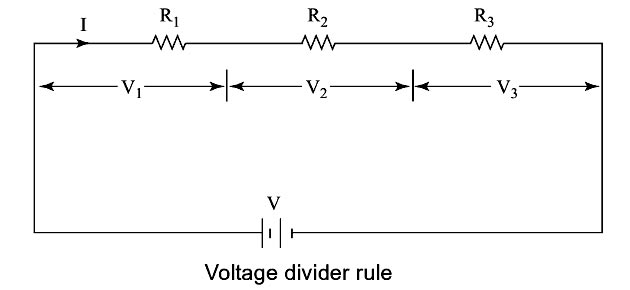
Ques.43. What will be the voltage across Resistance R2 in the circuit given below? (SSC 2016, Set-1)
14.35
13.33
15.45
12.33
Answer.2. 13.33
Explanation:-
The voltage across the resistance R2 can find out by voltage divider rule.
Voltage Divider Rule (VDR)
Voltage divider rule provides a useful formula to determine the voltage across any resistor when two or more resistors are connected in series with a voltage source. The voltage across the individual resistors can be given in terms of the supply voltage and the magnitude of individual resistances as follows
I = V ⁄ (R1 + R2 + R3)
V1 = I.R1 = V.R1 ⁄ (R1 + R2 + R3)
Similarly
V2 = I.R2 = V.R2 ⁄ (R1 + R2 + R3)
Hence for the given question the voltage across the resistance R2
V2 = V.R2 ⁄ (R1 + R2)
V2 = 20 × 40 ⁄ (20 + 40)
V2 = 13.33 Volt
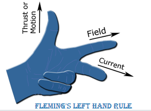
Ques.44. Fleming’s left-hand rule is used to find (SSC 2016, Set-1)
The polarity of the magnetic pole
The direction of flux in a solenoid
The direction of the magnetic field due to a current-carrying conductor in a magnetic field
The direction of the force on a current-carrying conductor in a magnetic field
Answer.4. The direction of the force on a current-carrying conductor in a magnetic field
Explanation
Force on a straight conductor carrying current placed in a magnetic field can be found by using Fleming’s left-hand rule.
The forefinger represents the direction of the magnetic field, the thumb represents the direction of the motion of the conductor and the middle finger Ives the direction of the current.
Ques.45. In a purely inductive circuit (SSC 2016, Set-1)
Current leads voltage by 90°
Current lags voltage by 90°
Current and voltage are in the same phase
Any of the above
Answer.2. Current lags voltage by 90°
Explanation:-
In a purely inductive circuit, the rate of change of current is opposed by the reactance of the coil, and the effect of this opposition is to make the current lag behind the applied voltage or be out of phase by 90°. The waveforms of current and voltage in a purely inductive circuit are shown in Fig.
The current lags the voltage by 90°, as V has reached its maximum at point A when current is zero at point B.
Ques.46. During discharge of a battery (SSC 2016, Set-1)
The voltage of the cell increases
The voltage of the cell decreases
The voltage remains the same
None of the above
Answer.2. The voltage of the cell decreases
Explanation:-
Battery cycle and depth of discharge One discharge and charge period are referred to as a battery cycle. A major factor affecting battery life is the depth of discharge i.e. how much the battery is discharged and how often. The depth of discharge of a battery is a measure in the percentage of the amount of energy which can be removed from a battery during a cycle. Limiting the depth of discharge will make the battery last longer. If discharged beyond its recommended depth of discharge, the life of a battery will be considerably reduced. As the rate of discharge is increased, the cell terminal voltage, that is, the voltage at the output terminals of the cell drops because of the internal resistance results in voltage drops within the cell due to the flow of current from the cell. These losses result in increased internal heating within the cell and reduced available energy.
It is suggested that lead-acid batteries not be discharged beyond 80%, even if the battery is designed for deep discharge. Lead-acid batteries that are deeply discharged may suffer from a permanent loss of capacity due to sulphation, acid dilution and the greater tendency for freezing. The fully charged lead-acid cell has 2.25 Volts. 80% of this voltage is nearly 1.8 Volts.
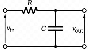
Ques.47. If an input signal with a non-zero direct current (dc) component is applied to a low pass RC network, then the D.C component in the output signal will be (SSC 2016, Set-1)
More than the input
Same as the input
Less than the input
Zero
Answer.3. Less than the input
Explanation:-
In electrical engineering, a filter is a frequency-selective circuit that passes a specified band of frequencies and blocks or attenuates signals of frequencies outside this band. These signals are usually voltages.
Passive Filter:- Filters that employ only passive elements such as capacitors, inductors, and resistors are called passive filters. In low-frequency applications (up to 100kHz), passive filters are generally constructed using simple RC (Resistor-Capacitor) networks, while higher frequency filters (above 100kHz) are usually made from RLC(Resistor-Inductor-Capacitor) components.
Active Filter:- When we apply a voltage across them or pass a current through them, they react in a certain orderly way according to simple rules, such as Ohm’s Law. They do not amplify the input signal, therefore, their output level is always less than the input.
Filters that make use of the properties of op-amps in addition to resistors and capacitors are called active filters such as Amplifier, transistor. Active components, such as transistors and op-amps, behave in a more complicated way and can have an amplifying effect on the current passed through them and the voltage applied across them.
Both active and passive filters are used in electronic circuits. However, active filters offer the following advantages over passive filters:
The flexibility of gain and frequency adjustment: Since op-amps can provide a voltage gain, the input signal in active filters is not attenuated as it is in passive filters. It is easy to adjust or tune active filters.
No loading effect: Because of the high input resistance and low output resistance of op-amps, active filters do not cause the loading of the input source or the load.
Cost and size: Active filters are less expensive than passive filters because of the availability of low-cost op-amps and the absence of inductors.
Parasitics: Parasitics are reduced in active filters because of their smaller size.
Digital integration: Analog filters and digital circuitry can be implemented on the same IC chip.
Filtering functions: Active filters can realize a broader range of filtering functions than passive filters.
Gain: An active filter can provide gain, whereas a passive filter often exhibits a significant loss.
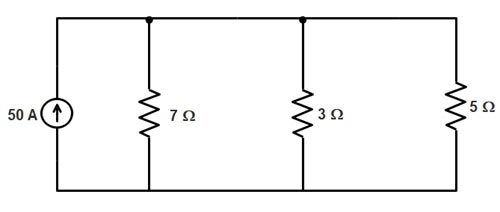
Ques.48. Determine the current flowing through the 7-Ω and 3Ω and 5Ωresistors, respectively in the following circuit (SSC 2016, Set-1)
5A, 4.8 A, 12 A
10.56 A, 24.64A and 14.79A
11.254 A, 9.582 A, 7.36A
2A, 4A , 4.56A
Answer.2. 10.56 A, 24.64A and 14.79A
Explanation:-
By applying the current division rule in the given circuit to find the current in the 7-Ω resistance
I1 = I × (R2R3) ⁄ (R1R2 + R2R3 + R3R1)
I1 = (50 × 3 × 5) ⁄ (7 × 3 + 3 × 5 + 5 × 7)
I1 = 750 ⁄ 71 = 10.56 A
current in the 3-Ω resistance
I2 = I × (R1R3) ⁄ (R1R2 + R2R3 + R3R1)
I2 = (50 × 7 × 5) ⁄ (7 × 3 + 3 × 5 + 5 × 7)
I2 = 1750 ⁄ 71 = 24. 64A
current in the 5-Ω resistance
I3 = I × (R1R2) ⁄ (R1R2 + R2R3 + R3R1)
I3 = (50 × 7 × 3) ⁄ (7 × 3 + 3 × 5 + 5 × 7)
I3 = 1050 ⁄ 71 = 14.79 A
Ques.49. A potential divider is normally connected (SSC 2016, Set-1)
At a distance V/100 meters from the generator where V is the voltage to be measured KV
Outside the generator circuit towards the load circuit
Within the generator circuit
None of these
Answer.2. Outside the generator circuit towards the load circuit
Explanation:-
A potential divider is a resistor network that produces a fixed or variable potential (voltage). This potential is lower than the potential of the supply.
A voltage divider (or potential divider) is a series circuit that is used to provide two or more reduced voltages from a single input voltage source.
Essentially, a potential divider consists of two resistors connected in series. Assuming that no current flows out of the divider at the junction of R1 and R2, the same current, I, flows through both resistors.
Ohm’s law applies to each resistor. For R2:
i = Vout/R2
Ohm’s Law also applies to the two resistors when connected in series:
i = VlN/(R1 + R2)
Combining these two equations:
VOUT/R2 = VlN/(R1 + R2)
VOUT = VIN × R2/(R1 + R2)
This equation states that the output voltage is directly proportional to the input voltage and the ratio of R1 and R2.
Effect of Load
The foregoing calculation assumes that no current flows out of the output terminal. However, the current is drawn from the output in most practical circuits. This is what happens:
Current I pass through R1. At the output of the divider, a current ILOAD passes through the load while the remainder I2passes on through R2. The diagram shows that R2 and the load (RLOAD) are resistances in parallel.
If R2 and the load are resistances in parallel, their combined resistance is less than the resistance of either of them separately. Therefore the PD across R2 is less when the load is connected. The measured value of Vout is less than expected.
Loading a voltage divider has the following effects:
(i) The output voltage is reduced depending upon the value of load resistance RL.
(ii) The current drawn from the source is increased because the total resistance of the circuit is reduced. The decrease in total resistance is due to the fact that loaded voltage divider becomes the series-parallel circuit.
(iii) The voltage divider should always be connected outside the generator circuit towards the load circuit (Test object) for accurate measurement.
Ques.50. Internal heating of the capacitor is usually attributed to (SSC 2016, Set-1)
Leakage resistance
Dielectric charge
Plate vibration
Electron Movement
Answer.1. Leakage resistance
Explanation:-
Leakage Resistance of a Capacitor
Consider a capacitor charged by a de voltage source. After the charging voltage is removed, a perfect capacitor would hold its charge indefinitely Because there is no such thing as a perfect insulator, however, the charge stored in the capacitor will eventually leak or bleed off, thus neutralizing the capacitor. There are three leakage paths through which the capacitor might discharge:
Leakage through the dielectric
Leakage across the insulated case or body between the capacitor leads
Leakage through the air surrounding the capacitor.
For paper, film, mica, and ceramic, the leakage current is very slight, or inversely, the leakage resistance is very high. The leakage resistance is much less for larger capacitors, such as electrolytic Capacitors. In general, the larger the capacitance of a capacitor, the lower its leakage resistance. Note that the leakage current in capacitors is fairly temperature-sensitive. The higher the temperature, the greater the leakage current (because of lower leakage resistance). The I2R loss is produced due to that leakage resistance. Hence, the internal loss happens due to the leakage power loss inside the capacitor.
The temperature at which the dielectric operates is a function of the ambient temperature in which the capacitor is located; the heat which is radiated or conducted to the capacitor; the internal heating of the capacitor due to power losses in the conductors and dielectric; the physical construction and thermal conductivity of the materials inside the capacitors; the transfer of heat internally by conduction and convection to the container; and the heat loss from the container by convection, conduction, and radiation.