Ques.91. Cutting pliers used for electrical work must have
High strength
Insulation✓
Non corrode
Sharp
The cutting pliers used for electric work should be provided with the insulating material such as plastic, Rubber etc. so that the person can be remain save from the electric shock.
Ques.92. The unit of luminous flux is
Steradian
Candela
Lumen✓
Lux
The luminous flux, which is also a photometric quantity, represents the light power of a source as perceived by the human eye. The unit of luminous flux is the lumen (Im).
It is defined as follows: a monochromatic light source emitting an optical power of (1, 683J watt at 555 nm has a luminous flux of 1 lumen (Im). The lumen is an SI unit.
Ques.93. A zero watt Lamp consumes
No power
About 5 to 7 W power✓
About 15 to 20 W power
About 25 to 30 W Power
Zero watt Night Lamp is a Low incident light bulb this bulb requires a very low current i.e around (0.023 A) and the power consumption is also very low 3 – 7 W.
In earlier days the analog electric energy meter was not very efficient to sense or measure zero-watt bulbs, therefore the meter uses to show zero or no consumption.
Ques.94. A DC generator used for ARC welding should have
Rising characteristics
Dropping Characteristics✓
Straight characteristics
None of these
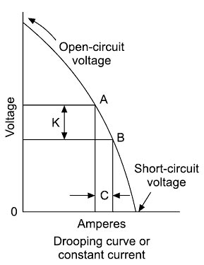
V-I Characteristics of an ARC Welding
Volt-ampere or V.I. characteristics of a welding plant have a great effect on the process of welding as different welding processes use welding plants with different V.I. characteristics. The V.I. characteristics indicate the relationship between the arc voltage and the arc current. During welding, the arc length between the electrode tip and the workplace determines the arc resistance and consequently the potential drop across the arc.
In other words, the arc length determines the arc voltage. Longer the arc, the higher the arc voltage. And it is this voltage that permits a certain flow of current according to the characteristics of the welding plant. A DC generator used for ARC welding should have dropping Characteristics.
The three main types of welding plant characteristics are:
Drooping (or Constant current) type
Flat (or Constant voltage) type
Rising voltage type.
Constant current (drooping voltage) output is preferred for manual arc welding because small variations in voltage caused by variations in arc length, do not significantly affect the current output and deposition rate. A DC generator is driven by a prime mover (electric motor or diesel engine) which produces DC current in either or reversed polarity. The current supplied by DC generator is alternating that can be converted to direct quantity by the use of a commutator.
The differential compound DC generator is used as a welding generator since it has drooping volt-amp characteristics. As the load current increases, the net flux due to the series and the shunt fields in opposition decrease and hence the generated EMF.
Ques.95. The welding electric circuit is ______
Always Earthed✓
Never Earthed
Through cables Only
None of these
The welding electric circuit is always earthed. Generally, welding and thermal cutting operations are not hazardous but complete safety is necessary for welding because electric current or high voltage current is used in it. The hazards which are more or less peculiar to welding are:
Electric Shock
Arc radiation
Fumes and dust Compressed Gases
Fire and explosions
Electric Shock
Electric shock may occur in welding if a current happens to pass through the welder body. The magnitude of the current will depend upon the resistance offered by the body. A current of 0.1 A or above, be it ac. or d c. is taken to be lethal to humans. Since the maximum human body resistance is 600 ohm, the lethal current will be provided by the voltage of just 60 V (V = ± R).
Electric shock results in many accidents that occur during welding. Therefore necessary precautions must be taken to minimize electric risk. This can best be done by ensuring the props insulation of cables, and reliable earthing o welding equipment. The grounding circuit sanitary sewers and water pipes or metallic structures of buildings and process equipment should never be used as earth or return for a welding circuit.
Ques.96. Direct resistance heating is used in
Electrode Boiler
Salt-Bath furnace
Resistance Welding
All of the above✓
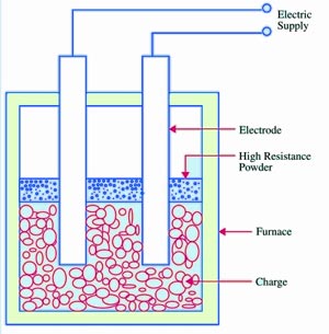
Direct resistance heating (or ohmic heating) is based on the flow of an electrical current through the body to be heated, which is directly connected to an electrical supply. The heating can be realized by DC or AC currents, but the industrial applications are mostly done with the alternating ones.
Materials with fairly high electrical resistivity, such as carbon and low alloy steels and nickel alloys, are readily heated by direct resistance. With low resistivity materials such as copper and aluminum, the process is often not cost-effective.
Direct resistance heating is used in the iron and steel industry: for heating rods and billets prior to rolling and forging for ferrous and non-ferrous annealing; either alone or i^l combination with other fuels for melting glass; in electrode boilers, for water heating and steam raising; and in salt baths for the surface heat treatment of metallic components.
Ques.97. The main drawback of resistance welding is
High initial as well as High maintenance cost✓
Difficult shapes and sections cannot be welded
Only similar metals can be welded
None of these
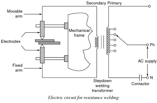
Resistance Welding
Resistance welding is the process of joining two metals together by the heat produced due to the resistance offered to the flow of electric current at the junctions of two metals. The heat produced by the resistance to the flow of current is given by:
H = I2Rt
where I is the current through the electrodes R is the contact resistance of the interface t is the time for which current flows.
Here, the total resistance offered to the flow of current is made up of:
(i) The resistance of the current path in the work.
(ii) The resistance between the contact surfaces of the parts being welded.
(iii) The resistance between electrodes and the surface of parts being welded.
In this process of welding, the heat developed at the contact area between the pieces to be welded reduces the metal to plastic state or liquid state, then the pieces are pressed under high mechanical pressure to complete the weld. The electrical voltage input to the welding varies between 4 and 12 V depending upon the area, thickness, composition, etc. and usually power ranges from about 60 to 180 W for each sq. mm of the area.
The electrical circuit diagram for the resistance welding is shown in Fig. This method of welding consists of a tap-changing transformer, a clamping device for holding the metal pieces, and some sort of mechanical arrangement for forcing the pieces to form a complete weld.
Advantages
The welding process is rapid and simple.
Localized heating is possible if required.
No need for using filler metal.
Both similar and dissimilar metals can be welded Comparatively lesser skill is required.
The maintenance cost is less.
It can be employed for mass production.
Disadvantages
The initial cost is very high.
High maintenance cost.
The workpiece with heavier thickness cannot be welded since it requires a high input current.
Applications
It is used by many industries manufacturing products made up of thinner gauge metals.
it is used for the manufacturing of tubes and smaller structural sections.
Ques.98. The process of adding, impurities to a semiconductor is known as ___
Polling
Intrusion
Pugging
Doping✓
In order to change the properties of intrinsic semiconductors a small amount of some other material is added to it. The process of adding other material to the crystal of intrinsic semiconductors to improve its conductivity is called doping. The impurity added is called dopant. The doped semiconductor material is called extrinsic semiconductors.
The doping increases the conductivity of the basic intrinsic semiconductors hence the extrinsic semiconductors are used in practice for the manufacturing of various electronic devices such as diodes, transistors, etc.
Depending upon the type of impurities, the two types of extrinsic semiconductors are,
N-TYPE
P-TYPE
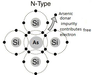
N-TYPE Impurity
The impurity material having five valence electrons is called the pentavalent atom. When this is added to an intrinsic semiconductor, it is called donor doping as each impurity atom donates one free electron to an intrinsic material. Such an impurity is called donor impurity. Examples of such impurities are arsenic, bismuth, phosphorous, Antimony, etc. This crests an extrinsic semiconductor with a large number of free electrons called an n-type semiconductor.
Germanium and Silicon are tetravalent. The impurity atoms may be either pentavalent or trivalent, i.e., from groups V and III of the periodic table. If a small quantity of a pentavalent impurity (having 5-electrons in tt outermost orbit) like Arsenic (As), Antimony (Sb), or Phosphorus (P) is introduced in Germanium, it replaces the equal number of Germanium atoms without changing the physical state of the crystal.
Each of the four out of five valency electrons of impurity says of Arsenic enters into covalent bonds with Germanium, while the fifth valence electron is set free to moo from one atom to the other as shown in Fig. The impurity is called donor impurity as it donates an electron and the crystal is called an N-type semiconductor.
A small amount of Arsenic (impurity) injects billions of free electrons into Germanium thus it creasing its conductivity enormously. In an N-type semiconductor, the majority carriers of charge are the electrons and holes as minority carriers. This is because when donor atoms are added to a semiconductor, the extra free electrons give the semiconductor a greater number of free electrons than it would normally have.
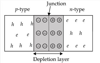
Ques.99. In a P-N junction, the potential barrier is due to the charges on either side of the junction. These charges are
Majority carriers
Minority carriers
Both majority as well as minority carriers
Fixed donor and acceptor ions✓
Let us now consider a p-n junction in which one side is a p-type semiconductor and the other side is an n-type semiconductor. The P side has a higher concentration of holes while the n-side has a higher concentration of free electrons. As a result, there is a tendency for the holes in the P-side to diffuse to the N-sides and the electrons in the N side to diffuse to the P-side. In a P-N junction, the potential barrier is due to the charges on either side of the junction. These charges are fixed donor and acceptor ions.
Formation of depletion region: The region on both the n- and P sides which are close to the junction develops a low concentration of charge carriers. This happens because, as the electrons on the N-side diffuse towards the p-side, they recombine with the holes close to the junction.
The same thing occurs with the hole diffusing from the p-side to the n-side. Since a large number of recombinations occur close to the junction, the charge carrier densities close to the junction decrease drastically. This region close to the junction is called the depletion region or depletion layer.
Creation of junction potential: The electric neutrality of the semiconductor material is disturbed in the region close to the junction because of the recombination which forms the depletion region. In the p-side of the depletion region, we have an accumulation of fixed negative charge ions since the atoms have acquired electrons from the n-region. Similarly, on the n-type side of the depletion region, there is an accumulation of fixed positive charge ions because the free electrons have moved to the p-region.
This double layer of positive and negative charges produces an electric field that exerts a force on the electrons and holes against their diffusion. The potential difference corresponding to this electric field is called the potential barrier (or junction potential or barrier potential VB). This name implies that this potential difference acts as a barrier against the diffusion of electrons and holes from their majority side to the minority side. The magnitude of this potential barrier is about 0.3 V in the case of germanium and about 0.7 V for silicon-based semiconductor diodes. The width of the depletion layer being of the order of one micron, the electric field that exists in the depletion layer is of the order of 105 Vm-1, which is indeed very high.
Ques.100. The ripple factor is
RMS value/DC Value✓
Peak Value/DC Value
Peak Value/RMS Value
RMS Value/Peak Value
Ripple factor gives an idea of the imperfection of d.c. signal. Periodical fluctuation or ripples are superimposed on the dc. signal. The ripple factor is defined as the ratio of the RMS value of an alternating component of load current or voltage to the average value of Load current or voltage
ϒ = VRMS ⁄ VDC = IRMS ⁄ IDC
For SSC JE 2017 Electrical paper with complete solutionClick Here
For SSC JE 2015 Electrical paper with complete solutionClick Here
For SSC JE 2014 (Evening shift) Electrical paper with complete solutionClick Here
For SSC JE 2014 (Morning shift) Electrical paper with complete solution Click Here
For SSC JE 2013 Electrical paper with complete solutionClick Here
For SSC JE 2012 Electrical paper with complete solutionClick Here
For SSC JE 2011 Electrical paper with complete solution Click Here
For SSC JE 2010 Electrical paper with complete solution Click Here
For SSC JE 2009 Electrical paper with complete solution Click Here