
Ques 5(a). What is loss load factor? Explain in detail how the loss load factor can be determined.
Answer:- Load factor is defined as the average load divided by the peak load in a specified time period say one month or one year
Load factor = Average load/ Maximum Demand
Annual Load Factor
The annual Load factor is the ratio of total energy production in a year to the total maximum demand over a year.
[latex display=”true”]{\text{Annual load Factor = }}\dfrac{{{\text{Annual Energy Production}}}}{{{\text{Annual Maximum Demand}} \times 8760}}[/latex]
Note:- In one year there are 8760 Hours.
A high load factor indicates efficient utilization of distribution assets while a low load factor shows inefficient utilization.A low load factor is therefore undesirable. Some forms of demand management, for example, demand shifting (described earlier under demand management), work on the principle of improving the load factor by delivering the same amount of energy at a lower peak demand.
Load Loss Factor
The load loss factor is the ratio of average power losses to the power losses at peak demand. As the load on the System varies. the losses vary too but the relationship between the losses is non-linear.
[latex display=”true”]{\text{Loss load Factor = }}\frac{{{\text{Average Power Losses}}}}{{{\text{Power Losses at Peak Demand}}}}[/latex]
It is understandable that there should be a relationship between system load factor which most utilities know and line losses, which are much harder to calculate.
Line losses, which are the sum of the I2R, or resistance losses, can be determined when the currents at peak load are known. Since the current in an electrical system varies with respect to time, there is no precise method to calculate losses over a period of time. However, it is done by multiplying peak loss by loss factor.
- In economic comparisons, it is often necessary to take account of the recurring annual system losses. System losses can be separated into so-called fixed losses and variable losses.
- The fixed losses are those due to the magnetization currents of such instruments like as transformers and reactors, which are often referred to as iron losses.
- For simplicity it is assumed that these losses occur for the full 8760 hours per annum, neglecting outages owing to maintenance or faulty.
- Where more accuracy is required, the effect of the variation of voltage on the lanes may need to be taken into account.
- The variable losses are those caused by the flow of current through the different items of equipment on the network and are also termed copper losses.
- Power losses in a component having resistance R are proportional to the square of the current flowing through it, i.e. Pi = I2R.

- If the load factor of a plant is 100%, the copper loss will be at its full value throughout the period and it is easy to Snd the cost of losses.
- In actual practice, the load factor is normally less than 100% and let this be F.
- It is difficult to evaluate copper losses over the year as they vary as the square of the square of the current and hence approximately as the square of the load, which in turn keeps on varying throughout the period.
- Therefore, the annual copper losses not only vary with the mean height of the annual load curve (ie., the load factor) but also upon its shape. For example, in Fig. the two load curves have a load factor of 50% but the losses in case of curve B are 1/4th that of curve A.
- There are only two possibilities by which accurate evaluation or measurement of loses can be done.
- The first of these is to obtain load curves for each day over the year and find the mean value of the squared ordinates. Thi seems quite difficult and laborious and therefore is not normally used.
- The other possibility is to measure, with some instrument, a quantity proportional to the integral of the current squared over the year which normally is not done.
- Moreover, these methods are not valid for a new installation as the shape of the load curve would not be known even though the load factor is known.
- Therefore an empirical formula, for estimating losses, is evolved using load factor. Say, I is the maximum current with load factor F.
- The greatest possible loss would occur if maximum current flows for a fraction F of the year and no current in the remaining part of the year.Under this condition, the loss would be proportional to I2F.
- In the second case, the least possible loss will occur, with the same load factor, if the mean current IF flows continuously except when a peak current “I” is reached momentarily as shown in Fig. when the copper loss could be considered negligible.Under this condition, the loss will be proportional to I2F2.
- flows continuously except when a peak current “I” is reached momentarily as shown in Fig. when the copper loss could be considered negligible.
- Now it is convenient to omit the factor I2 from both the cases and express the losses as the fraction of those which would occur if the maximum current flows continuously.
- This factor which is the load factor of losses (loss load factor) would then be “F” in the first and “F2” in the second case.
- In any given situation the losses would be somewhere. between these extreme situations and the most convenient to assume will be a load factor of 50% as in Fig.
- It gives a simple formula for the loss factor as
G = 0.5 F + 0.5 F2
But generally, in practice, the Peak load occurs for a relatively short time and the above formula seems to give the relatively high value of the loss.
A better approximation could be that three-tenths of the consumption takes place at maximum load and the remainder at the mean load This gives the loss factor as
G = 0.23 F + 0.75 F2
or
G = 0.23 × (Load Factor) + 0.75 × (Load Factor)2
Ques 5(b). Discuss the various busbar system for the distribution networks.
Answer:- Bus -Bar term is used as a main bar or conductor carrying an electric current to which many connections may be made. The term bus is derived from the word omnibus, meaning collector of things. Thus electrical bus-bar is the collector of an electric circuit of electrical energy at one location.
Bus Bar Arrangement
There are several types of bus bar arrangements. To decide a particular arrangement various factors are to be considered. These factors are system voltage, flexibility, the reliability of supply, the position of the substation in the system and cost.
Following points are to be considered while selecting bus bar arrangement*
- The bus bar arrangement should be simple.
- The maintenance of the system should be possible without interruption of supply
- It should not provide any danger to operating personnel while doing maintenance or repair.
- The layout should accommodate the future expansion with increase in load demand.
- It should be economical one in view of reliability and continuity of supply.
Following are the bus bar arrangements used in the substation
- Single bus bar system
- Single bus bar system with sectionalization
- Main and transfer bus system
- Double-bus bar system with single breaker or duplicate bus bar system
- Double-bus bar system with double breaker
- Breaker and half system with two main buses
- Ring bus bar system
Single Bus Bar System
This is the simplest and cheapest bus bar arrangement shown in the Fig. It consists of a single bus bar to which all incoming and outgoing lines are connected. It requires less maintenance. But the maintenance and repair are not possible without interruption of supply. Also the extension is not possible without a shutdown.
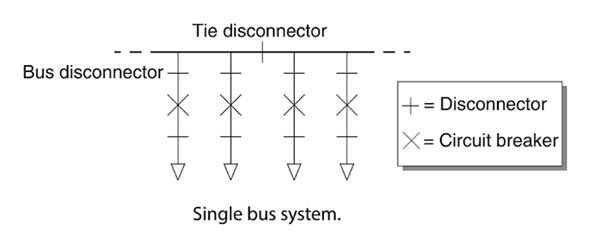
This system is used for the system voltages upto 33 kV. The indoor 11 kV substations always use this arrangement. As the connections of the equipment are simple, the system is convenient to operate. This arrangement is used where relative importance of substation is less.
Thee are two incoming lines connected to bus bars through isolators and circuit breakers. The outgoing lines are connected to the bus bars through the transformers.
Advantages
- The operation of the system is simple.
- It has low initial cost.
- It has the low maintenance cost.
Disadvantages
- In case of a fault, the complete system will be switched off.
- In case of maintenance, continuity of supply will be interrupted.
- The system is not reliable.
- Without a complete shutdown, it is impossible to go ahead with future expansion.
Single bus bar system with sectionalization
In this type of busbar arrangement, the circuit breaker, and isolating switches are used.The sectionalization of the bus bar ensures continuity of supply on the other feeders, during the time of maintenance or repair of one side of the bus bar. The whole of the supply need not be shut down. The number of sections of a bus bar is usually 2 or 3 is a substation but actually, it is limited by the short-circuit current to be handled.This type of arrangement uses one addition circuit breaker with low breaking capacity, hence making the system cost efficient.
As in single bus bar system with sectionalization, the bus bar is divided into sections. Hence, each section will work as a separate bus bar and the equipment are connected to all the sections. Hence, the load is distributed equally. Any section can be connected by closing the circuit breaker and isolator. This type of syste is used for 33 kV.
Advantages
- The operation of this system is simple as in case of the single bus bar.
- The maintenance cost of this system is comparable to the single bus bar.
- For maintenance or repair of the bus bar, only one half of the bus bar is required to be de-energized. So complete shut down of the bus bar is avoided.
- It is possible to utilize the bus bar potential for line relays.
Disadvantages
- In case of a fault on the bus bar, one half of the section will be switched off.
- For regular maintenance also, one of the bus bars is required to be de-energized.
- For maintaining or repairing a circuit breaker, it is required to be isolated from the bus bar.
Double Bus Bar System
This system is shown in Fig. It consists of two identical bus bars, one is the main bus bar and another one is spare bus bar. Each bus bar has the capacity to take up the entire substation load. Each load may be fed from either bus bar. The infeed and load circuits can be further divided into two separate groups based on operational considerations (maintenance or repair). Any bus bar may be taken out for maintenance and cleaning of insulators.
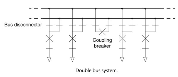
With the help of bus coupler, the incoming and/or outgoing lines are connected to any bus bar through isolator and circuit breaker. This system is adopted when the voltage is greater than 33 kV. This arrangement does not permit breaker maintenance without causing the interruption in supply.
Advantages
- Permits some flexibility with two operating buses.
- Any main bus may be isolated for maintenance.
- The circuit can be transferred readily from one bus to another by using bus coupler and bus-selector disconnect switches.
- The maintenance cost of the arrangement is less.
- The potential of the bus is used for the operation of the relay.
- The load can easily be shifted on any of the buses.
Disadvantages
- The cost of this scheme is high. So it can be used where loads and continuity of supply are the main considerations than the cost. For voltages beyond 33 kV duplicate bus bar system is frequently used.
- The breaker in the bus coupler section provides on load change over from one busbar to the other. The normal bus section isolators cannot be used for breaking load currents. This scheme does not provide any means for the breaker Maintainance without interrupting the supply.
Breaker-and-a-half scheme
The scheme shown in Figure. provides for two main buses, both normally energized. Between the buses are three circuit breakers and two circuits. This arrangement allows for breaker maintenance without interruption of service. A fault on either bus will cause no circuit outage. A breaker failure results in the loss of two circuits if a common breaker fails and only one circuit if an outside breaker fails. Fewer breakers are needed for the same flexibility as in the double-breaker system.
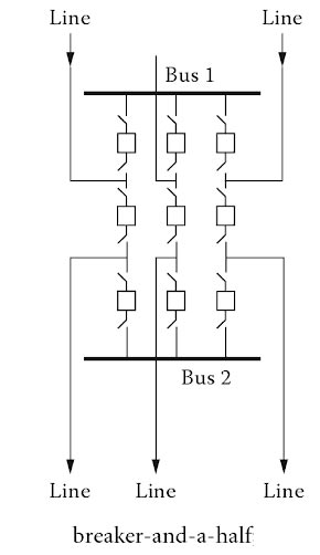
Advantages
- This system is more economical as compared to a double-bus double breaker arrangement.
- A fault in a breaker or in a bus will not interrupt the supply.
- Addition of circuits to the system is possible.
- High reliability.
- Any main bus can be taken out of service at any time for maintenance.
Disadvantages
- 3/2 breaker per circuit.
- The relaying becomes more complicated as compared to that in a single-bus arrangement.
- The maintenance cost is higher.
Ring Bus Bar System
In this arrangement, there are two ways to supply to each circuit. Hence, if any circuit breaker is disconnected for maintenance, the supply is maintained through the other path. However, two CT is required for each circuit and hence the overall cost of the system increases. For more than six circuits, this type of system is not suitable. The single line diagram of this busbar arrangement is shown in Fig
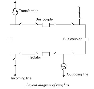
Advantages
- The reliability of this system is more because the power can be supplied through the other path.
- When one circuit is taken for maintenance, the supply is maintained through the other circuit.
- The maintenance of any circuit breaker is possible without interrupting the power supply.
Disadvantages
- The only disadvantage is that two CTs are required which increase the cost of the system.
Ques 6(a). Draw the output characteristics of the common emitter transistor. Show various region of operation of BJT on this characteristics. Describe the application of operating the BJT into the different region.
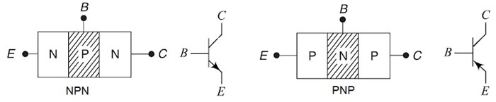
Answer:- A Bipolar Junction Transistor (BJT) is a three-layer, two junction semiconductor device consisting of either two N-type and one P-type layer of material (NPN transistor) or two P-type and one N-type layer of material (PNP transistor). If a thin layer of N-type Silicon is sandwiched between two layers of P-type silicon. This transistor is referred to as PNP. Alternatively, in an NPN transistor, a layer of P-type material is sandwiched between two layers of N-type material.
The term bipolar is to justify the fact that holes and electrons participate in the injection process into the oppositely polarised material. If only one carrier is employed (electron or hole). it is considered a unipolar device.
Transistor Biasing
Usually, the emitter-base junction is forward biased and the collector-base junction is reverse biased. Due to the forward bias on the emitter-base junction, an emitter current flows through the base into the collector. Though the collector-base junction is reverse biased, almost the entire emitter current flows through the collector circuit.
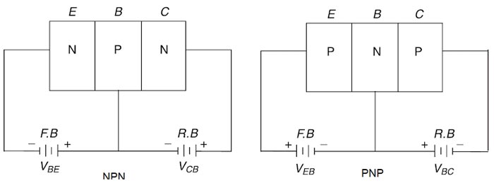
Operation and Current Components of NPN Transistor
The forward bias applied to the emitter-base junction of an NPN transistor causes a lot of electrons from the emitter region to crossover to the base region. As the base is lightly doped with the P-type impurity, the number of holes in the base region is very small and hence the number of electrons that combine with holes in the P-type base region is also very small. Hence a few electrons combine with holes to constitute a base current IB. The remaining electrons (more than 95%) crossover into the collector region to constitute a collector current IC. Thus the base and collector current summed up gives the emitter current, i.e IE = – (IC + IB)
In the external circuit of the NPN bipolar junction transistor, the magnitudes of the emitter current It the base current IB and the collector current IC are related by IE = IC + IB
CIRCUIT CONFIGURATION OF A BIPOLAR JUNCTION TRANSISTOR
A transistor has three terminals: an emitter (E), base (B) and collector (C) and two junctions such as emitter-base junction and collector-base junction. Each of these junctions requires two terminals for a biasing arrangement. When a transistor is connected in a circuit, it requires four terminals, i.e. two input terminals and two output terminals. Therefore, one of the three transistor terminals (emitter, base, and collector) is used as a common terminal between input and output. Depending upon the common terminal, the transistor may be connected to the three different configurations such as common emitter (CE), common base (CB) and common collector (CC) configurations.
The common emitter terminal configuration can be considered the fundamental building block of BJT analog amplifier circuits. The common base and common collector are applied to some extent in more special-purpose roles, such as for high output resistance (common base) and low output resistance (common collector). Therefore, a study of the transistor in the common-emitter mode is basic to a study of analog circuits.
Common Emitter Configuration:
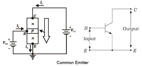
In the common-emitter configuration, the emitter of a transistor is connected to a common terminal between input and output as shown in Fig. The input signal is applied between the emitter and base terminals. The output will be obtained from the collector and emitter terminals. The common emitter configuration of the transistor is the most commonly used one in circuits.
Common Emitter Current Gain β
The current gain, beta (β), is defined for the common-emitter configuration of a BJT and can be defined in two forms: the dc current amplification factor (βdc) and the ac current amplification factor (βac).
The dc current gain βdc is defined as the ratio of collector current to base current at a constant VCE under dc biasing conditions.
[latex display=”true”]{\beta _{dc}} = \dfrac{{{I_C}}}{{{I_B}}}[/latex]
Similarly, the ac current gain, βacis defined as the ratio of change in collector current to a corresponding change in base current at a given VCE under ac signal conditions.
Since the collector current is the output current for a common-emitter configuration and the base current is the input current.
[latex display=”true”]{\beta _{ac}} = \dfrac{{{I_C}}}{{{I_B}}}[/latex]
A common-emitter configuration offers the following characteristics:
- The transistor circuit will have a moderately high input impedance
- Low output impedance
- Moderately high current gain
- Moderately high voltage gain and very good and wide range of frequency response and hence find dominant applications in voltage, current and power amplifiers.
Relation between α and β
[latex display=”true”]\begin{array}{l}{I_E} = {I_B} + {I_c}\\\\\dfrac{{{I_c}}}{\alpha } = \dfrac{{{I_c}}}{\beta } + {I_c}\\\\{\text{Dividing both sides of the equation by }}{I_c}\\\\\dfrac{1}{\alpha } = \dfrac{1}{\beta } + 1\\\\{\text{On Solving}}\\\\\alpha = \dfrac{\beta }{{\beta + 1}}\\or\\\\\beta = \dfrac{\alpha }{{1 – \alpha }}\end{array}[/latex]
Characteristics of Common Emitter Configuration
To determine the characteristics of a transistor in common emitter (CE) configuration, the circuit is arranged as shown in Figure. The base of the emitter voltage VBE can be varied by adjusting the potentiometer R1. Whereas, the collector to emitter voltage can be varied by adjusting the setting of potentiometer R2. For different settings, the currents and voltage are read from the milliammeter and voltmeter. On the basis of these readings, the input and output characteristic curves are plotted on the graph.
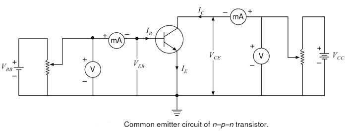
Input Characteristics:
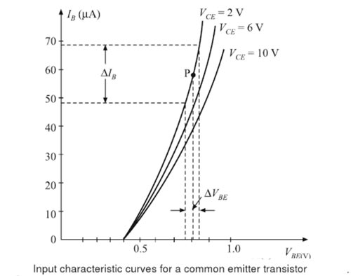
In common emitter configuration, the curve plotted between base current IB and base-emitter voltage VBE is called input characteristics. For determination of input characteristics, collector-emitter voltage VCE is held constant, and base current IB is recorded for different values of base-emitter voltage VBE. Now, the curves are drawn between base current IB and base-emitter voltage VBE for different levels of VCE as shown in Figure. The following are the main points regarding input characteristics:
- These curves are similar to those obtained for common base (CB) configuration, i.e., like a forward diode characteristic. The only difference is that in this case, IB increases less rapidly with increase in VBE. Hence, the input resistance of CE configuration is comparatively higher than that of CB configuration.
- The change in VCE does not result in a large deviation of the curves and hence the effect of the change in VCE on the input characteristics is ignored for all the practical purposes.
Input resistance
The ratio of change in base-emitter voltage (ΔVBE) to the resulting change in base current (ΔIB) at the constant collector-emitter voltage (VCE) is known as input resistance, i.e.,
Input resistance RI = (ΔVBE)/(ΔIB) at constant VCE.
In common emitter configuration, the typical value of input resistance is of the order of a few hundred ohms.
Output Characteristics:
The output characteristics of a common emitter transistor are the curve drawn between collector current lC and collector-emitter voltage VCE for a given value of base current IB. For the determination of common emitter output characteristics, base current IB is maintained constant at several convenient levels. At each fixed level of IBM collector-emitter voltage VCE is adjusted in steps, and the corresponding values of collector current lc are noted. For each level of IB, IC is plotted versus VCE. Thus a family of characteristics is obtained (Figure). The main points regarding output characteristics are as follows:
(i) In the active region, Ic increases slightly as VCE increases. The slope of the curve is a little bit more than the output characteristics of the common base (CB) configuration. Hence, the output resistance (ro) of this configuration is less as compared to the CB configuration.
(ii) Since the value of Ic increases with the increase in VCE at constant IB, the value of, β also increases (β = IC/IB).
(iii) When VCE falls below the value of VCE (i.e., below a few tenths of a volt). IC decreases rapidly. In fact, at this stage, the collector-base junction is also forward biased and the transistor works in the saturation region. In the saturation region, lC becomes independent, and it does not depend upon the input current IB.
(iv) In the active region lc = BIB, hence, a small current IC is not zero, but its value is equal to the reverse leakage current ICEO (i.e., collector to emitter current when the base is open).
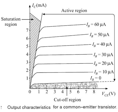
Output resistance
The ratio of change in the collector-emitter voltage (ΔVCE) to the change in collector current (ΔIC) at the constant base current IB is called output resistance (Ro), i.e.,
Output resistance Ro = ICE (at constant IB)
The output resistance of the CE configuration is less than the CB configuration as the slope of output characteristics is more in this case. Its value is of the order of 50 kΩ.
Active Region
In the active region, the collector junction is reverse biased and the emitter junction is forward biased. In the output characteristics, the active region is the area to the right of the ordinate VCE = a few tenths of a volt and above IB = 0. In this region, the transistor output current responds most sensitively to an input signal. If the transistor is to be used as an amplifying device without appreciable distortion, it must be restricted to operate in this region.
In the active region, IC is practically independent of VCE and is determined only by lE.The active region lies between cutoff and saturation points.
Cut-off Region
The region of the output characteristics where both the junctions (emitter and collector) are reverse biased, is known as the cutoff region of the transistor.
In order to cut-off the transistor, it is not enough to reduce lB to zero. Instead, it is necessary to reverse bias the emitter junction slightly. The cut-off is thus defined as the condition where the collector current is equal to the reverse saturation current ICO and the emitter current is zero.
Saturation Region
The region of the output characteristics where both junctions (emitter and collector) are forward biased, is known as the saturation region of the transistor. The saturation region lies very close to the zero of the collage axis where all curves coincide and fall quickly towards the origin. The saturation can be considered to occur at the knee of the curve.
In the saturation region, the collector junction (as well as the emitter junction) is forward biased by at least the entire voltage. The saturation region is very close to the zero voltage axis where all the curves merge and fall rapidly toward the origin. In the saturation region, the collector current is approximately independent of base current. In saturation, the collector current is nominally VCC/RL where VCC is the voltage applied at the collector junction and RL is the load resistance.
[ninja_tables id=”27864″]
Ques 6(b). Describe the law of illumination and their actual limitations in actual practice.
Answer:-
Illumination: It is the luminous flux received by a surface per unit area. It is denoted by
symbol E and is measured in ‘lumen per square meter ‘or lux or ‘meter-candle’ (i.e., E = F/A lumens/m2 or lux, where A is the area of the surface).
Illumination differs from light very much, though generally these terms are used more or less synonymously. Strictly speaking, light is the cause and illumination is the result of the light on the surfaces on which it falls. Thus illumination makes surfaces more or less bright with a certain color and it is this brightness and color which the eye sees and interprets as something useful.
Laws of illuminations.
There are two laws of illuminations.
- Law of Inverse Squares
- Lambert’s Cosine Law
Law of Inverse Square
The relationship between distance and intensity of radiation is called the inverse square law because the intensity of radiation varies inversely as the square of the source film distance.
This is an important law of light that describes what happens to the intensity of light over distance. The law states that the quantity of light is inversely proportional to the square of its distance. That should clear things up!
Perhaps an example of how the inverse square law works is easier to comprehend. The inverse square law describes what happens to light as it spreads out over distance. Let’s say the proper aperture to use is f/16 when the flash is 4 feet away from the subject. If you cut the flash to subject distance in half to only 2 feet, you do not double the amount of light hitting the subject. Instead, you quadruple the amount of light or add 2 stops of light to the subject. Conversely, if you move the flashback to 8 feet from the subject (twice as far), the amount of light striking the subject is only 1/4 as much because the beam of light is spreading out rapidly so the intensity drops. If you move the flash to 16 feet from the subject, the amount of light drops another 2 stops for a total of 4 stops. As you can see, the light output of the flash rapidly drops as the distance to the subject increases which affects how you use flash tremendously.
The typical electronic flash won’t do you much good if the subject is 50 feet away since very little of the flash actually reaches the subject. That’s why flash photos often end up with a black background.
- As light radiates from a point source, the intensity of light (I) is inversely proportional to the square of the distance (d)from the source.
E ∝ I/d2
- As intensity is the power per unit area (W/m2), it naturally decreases with the square of the distance as the size of the radiative spherical wavefront increases with distance.
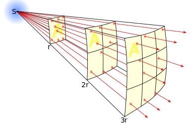
- Illumination of a surface is inversely proportional to the square of the distance between the surface and the light source provided that the distance between the surface and the source is sufficiently large so that the source can be regarded as a point source.
- A Source of light which emits light equally in all direction,
For Center of the hollow sphere.
- Light spreads uniformly mean light spreads the same in each direction.
- For Center of hollow large radius,
- Light spreads over a large area proportional to the square of the radius.
Conclusion:- As radius increases, it will be inversely proportional to the square of the distance.For Parallel Surface, (Cone or Pyramids)
Lambert’s cosine law
In optics, Lambert’s cosine law says that the radiant intensity observed from a “Lambertian” surface is directly proportional to the cosine of the angle θ between the observer’s line of sight and the surface normal. The law is also known as the cosine emission law or Lambert’s emission law. It is named after Johann Heinrich Lambert, from his Photometria, published in 1760.
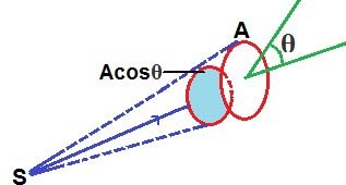
An important consequence of Lambert’s cosine law is that when such a surface is viewed from any angle, it has the same apparent radiance. This means, for example, that to the human eye it has the same apparent brightness (or luminance). It has the same radiance because, although the emitted power from a given area element is reduced by the cosine of the emission angle, the size of the observed area is decreased by a corresponding amount. Therefore, it! radiance (power per unit solid angle per unit projected source area) is the same For example, in the visible spectrum, the Sun is not a Lambertian radiator; it! brightness is a maximum at the center of the solar disk, an example of limit darkening. A black body is a perfect Lambertian radiator.
Hence Lambert’s Cosine Law states that when light falls obliquely on a surface, the illumination of the surface is directly proportional to the cosine of the angle θ between the direction of the incident light and the surface normal. The law is also known as the cosine emission law or Lambert’s emission law.
I ∝ Cosθ
⇒ The inverse square law is only applicable to the points on a surface that receives light rays from a source at right angles. However, lamps emit light at various angles, therefore the inverse square law needs to be corrected in order to study rays of light that are inclined.
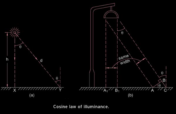
Figure “a” shows that light falls normally at X, but obliquely (inclined) at Y. The illuminance at X is greater than that at Y because distance “h” is less than distance “d”. Also, light falls on a greater area at Y. and therefore results in decreased illuminance.
Consider a beam of light, inclined at angle e to the normal. Draw line AB normal to the light rays.
In ΔABE (b), AC = AB/cosθ
This can also be written as
Area AC = Area AB/ Cosθ
When θ = 0°
Cos0° = 1
Therefore AC = AB = A1B1
When θ = 90°,
No point on the floor receives any light, as the light rays are horizontal.
For any angle between 0° and 90°, area AC will be greater than area AB.
When θ = 60°,
cosθ = 0.5;
Therefore AC = 2 AB.
The inverse square law (I/d2) is modified for light falling obliquely on a horizontal surface and is known as Lambert’s cosine law of illuminance:
[latex display=”true”]E = \dfrac{I}{{{d^2}}}\cos \theta—(1)[/latex]
From Figure “a”
[latex]\begin{array}{l}\dfrac{h}{d} = \cos \theta \\\\or\\\\d = \dfrac{h}{{\cos \theta }}\\\\or\\\\{d^2} = \dfrac{{{h^2}}}{{{{\cos }^2}\theta }} – – – – – – (2)\end{array}[/latex]
Combining equation 1 and 2
[latex display=”true”]\begin{array}{l}E = \dfrac{I}{{{h^2}}}{\cos ^3}\theta – – – – (3)\\\\{\text{Since Cos}}\theta {\text{ = }}\dfrac{h}{d}\\\\\therefore E = \dfrac{{Ih}}{{{d^3}}}\end{array}[/latex]
∴ I ∝ Cos3θ
I ∝ 1/d3
Equations 1 and 3 can be used to solve problems that involve light falling obliquely on surfaces.
For SSC JE CONVENTIONAL Paper 2017 CLICK HERE
For SSC JE CONVENTIONAL Paper 2016 CLICK HERE
For SSC JE 2017 Electrical paper with complete solution Click Here
For SSC JE 2015 Electrical paper with complete solution Click Here
For SSC JE 2014 (Evening shift) Electrical paper with complete solution Click Here
For SSC JE 2014 (Morning shift) Electrical paper with complete solution Click Here
For SSC JE 2013 Electrical paper with complete solution Click Here
For SSC JE 2012 Electrical paper with complete solution Click Here
For SSC JE 2012 Electrical paper with complete solution Click Here
For DMRC 2016 Solved Paper CLICK HERE
For DMRC 2015 Solved Paper CLICK HERE
For DMRC 2014 Solved Paper CLICK HERE
For NMRC 2017 Solved Paper CLICK HERE