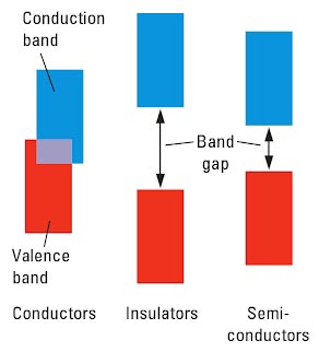
It is a gap between the valence band and conduction band where valence electrons in the conduction band get excited when they get sufficient energy and move to the valence band.
An energy band containing valence electrons is called the valence band. If the valence band is partially filled it requires very little added energy to excite a valence electron to a slightly higher energy orbital. Such a small increment of energy can be provided by applying an electric field, for example.
The band with the next higher average energy above the valence band is called the conduction band.
Insulators
Now consider the two outermost energy bands of a material in which the lower band is filled with electrons and the higher band is empty at K. The lower, filled band is called the valence band, and the upper, empty band is the conduction band. (The conduction band is the one that is partially filled in a metal.) It is common to refer to the energy separation between the valence and conduction bands as the energy gap Eg of the material.
The energy-band theory also explains why some solids are electrical insulators (or just insulators), that is, substances that do not conduct electricity. In an insulator, there is a large bandgap between the valence and conduction bands. Very few electrons have enough energy to move across the large gap from a filled lower energy band to an empty higher energy band, so no current flows through an insulator when an external electric field is applied.
Metals
In a metal, the valence band and the conduction band overlap, so electrons can move freely from the valence band to the conduction band this explains the high electrical conductivity of metals.A substance with overlapping valence and conduction bands is an electrical conductor (or just conductor).
When the conduction band is close in energy to the valence band, the electrons can absorb a wide range of wavelengths in the visible region of the spectrum. As the excited electrons fall back to their lower energy states, they emit their extra energy as visit light, producing the luster characteristic of metals.
Semiconductors
In a semiconductor, a narrow energy gap separates the valence band and the conduction band. At very low temperatures, electrons remain in the filled low energy valence band, and semiconductors are not good conductors. As temperature rises more electrons have enough energy to jump across the bandgap into the conduction band, so conduction increases.
A sufficiently large electric field also can provide the energy needed for electrons to jump the bandgap. This property of semiconductors— switch from insulator to conductor with the application of an external electric field the basis for the operation of transistors, the cornerstone of modern electronics.
Ques.142. The capacitance of a capacitor is ______ the distance between the metal plates.
Inversely proportional to✓
Independent of
Directly proportional to the square of
Directly proportional to
The capacitance of a parallel plate capacitor is given by,
C = εA/d
Where ϵ is dielectric constant
A is the area of the cross-section of the plates
d is the distance between the plates
The capacitance is inversely proportional to distance.
The capacitance C of a capacitor is the ratio of the magnitude of the charge on either conductor (plate) to the magnitude of the potential difference between the conductors (plates).
C = Q/V
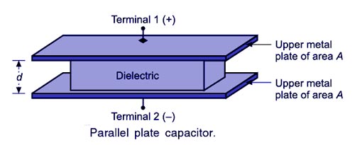
THE PARALLEL-PLATE CAPACITOR
The figure shows the structure of a parallel plate capacitor. It is made up of two parallel plates of the area of cross-section A, kept in an insulating medium and separated from each other by a distance of d meter. Then, if the two plates are applied with potential, one of the plates will be positively charged and the other negatively charged. Let the charge on the plates be given by Q coulombs.
The capacitance of a device depends on the geometric arrangement of the conductors. The capacitance of a parallel-plate capacitor with plates separated air can be easily calculated from three facts.
The magnitude of the electric field between two plates is given E = σ/εo, where σ is the magnitude of the charge per unit area on each plate and εο = Permittivity of free space = 8.85 × 10⁻¹²
Second, the potential difference between the two plates is ΔV = Ed, where d is the distance between the plates.
Third, the charge one plate is given by q = σA, where A is the area of the plate. Substituting the three facts into the definition of capacitance gives the desired result:
C = εA/d
Hence the capacitance of the capacitor is directly proportional to the area of plates and inversely proportional to the distance between the metal plates.
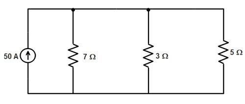
Ques.143. Determine the current flowing through the 7-Ω and 3Ω resistors, respectively in the following circuit
5A and 4.8 A
10.56 A and 24.64A✓
11.254 A and 9.582 A
2A and 4A
By applying the current division rule in the given circuit to find the current in the 7-Ω resistance
I1 = I × (R2R3) ⁄ (R1R2 + R2R3 + R3R1)
I1 = (50 × 3 × 5) ⁄ (7 × 3 + 3 × 5 + 5 × 7)
I1 = 750 ⁄ 71 = 10.56 A
current in the 3-Ω resistance
I2 = I × (R1R3) ⁄ (R1R2 + R2R3 + R3R1)
I1 = (50 × 7 × 5) ⁄ (7 × 3 + 3 × 5 + 5 × 7)
I1 = 1750 ⁄ 71 = 24. 64A
Ques.144. Which of the following statements is applicable for a three-phase AC circuit for a star connection?
Phase voltage is square root three times the line voltage and phase current is equal to the line current.✓
Phase voltage is equal to the line current and line current is equal to the phase voltage.
Phase voltage is equal to line voltage and phase current is three times the line current
Phase voltage is equal to the line voltage and line current is equal to the phase current
In star-connected load the phase voltage between the neutral point and any one of the line connections is 1/√3 × VL of the line voltage.
Therefore the line voltage is √3 times the phase voltage.
i.e VL = √3Vph
In star connection, the line current is equal to the phase current.
Ques.145. For a star connected load being measured for power by the two-wattmeter method, if W1 = VLILcos(30 − φ)and W2 = VLILcos(30 + φ), then the total 3-phase power will be:-
VLIL(2cos30°Cosφ) = √3VLILcosφ = total input power
Ques.146. The wattmeter method is used to measure the power in a three-phase load. The wattmeter readings are 400 W and −35 W. What will be the power factor?
0.85
0.9
0.43✓
0.635
As given in the above question
W1 = 400 W
W2 = −35 W
The power factor of the two wattmeters is
tanØ = √3[(W1 – W2) / (W1 + W2)]
tanØ = √3[(400 + 35]) ⁄ (400 − 35 W)]
Φ = 64°
Power factor = cosφ = cos64° = 0.43
Ques.147. Which of the following is NOT conductive material?
Copper
Germanium✓
Tungsten
Platinum
Germanium is a semiconductor material. If a small quantity of a pentavalent impurity (having 5-electrons in tt outermost orbit) like Arsenic (As), Antimony (Sb) or Phosphorus (P) is introduced in Germanium, it replaces the equal number of Germanium atoms without changing the physical state of the crystal.
Each of the four out of five valency electrons of impurity says of Arsenic enters into covalent bonds with Germanium, while the fifth valence electron is set free to moo from one atom to the other as shown in Fig. The impurity is called donor impurity as it donates an electron and the crystal is called an N-type semiconductor.
A small amount of Arsenic (impurity) injects billions of free electrons into Germanium thus it creasing its conductivity enormously. In an N-type semiconductor, the majority carriers of charge are the electrons and holes as minority carriers. This is because when donor atoms are added to a semiconductor, the extra free electrons give the semiconductor a greater number of free electrons than it would normally have.
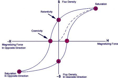
Ques.148. Which of the statements is correct for a permanent magnetic material?
The residual induction and the coercive field should be large✓
The area of the hysteresis loop should be small.
The initial relative permeability should be small.
The residual induction and the coercive field should be small.
Residual induction: Residual induction is the residual flux density remaining in a saturated magnetic material after the magnetizing force has been withdrawn. It represents the maximum flux output from the magnet that occurs at zero air gap.
or
The residual induction is any magnetic induction that remains in a magnetic material after removal of an applied magnetic field
Remanence: Remanence is defined as the magnetic induction that remains in a magnetic circuit after the withdrawal of an applied magnetizing force.
Coercive Force – The amount of reverse magnetic field which must be applied to a magnetic material to make the magnetic flux return to zero.
Properties of the material of a permanent magnet :
(1) It should have high retentivity so that it remains magnetized in the absence of the magnetizing field.
(2) It should have high saturation magnetization.
(3) It should have high coercivity so that it does not get demagnetized easily.
Hard magnetic materials have large hysteresis loss due to large hysteresis loop area.
In these materials, the domain wall movement is difficult because of the presence of impurities and crystal imperfections and it is irreversible.
The coercivity and retentivity are large.
Hence, these materials cannot be easily magnetized and demagnetizer
Hard magnetic materials are used to produce permanent magnets. Hysteresis losses are of no significance here as no repeated reversals of magnetization is involved in a permanent magnet. The permanent magnets must have high residual induction B. and large coercive field Hc. The area of the hysteresis loop between Br and Hc represents the energy required to demagnetize a permanent magnet. The maximum value of this area (= BrHr) called the energy product, must be as large as possible for permanent magnets.
As steel and alnico have high coercivity, therefore, they are used for making permanent magnets. The metals in Alnico magnets are indicated by the pairs of letters making up the name, Aluminum, Nickel, and Cobalt.
Ques.149. An alternating current is given by i = 100sin314t A. Its average value will be_______
70.7 A
63.7 A✓
100 A
50 A
The average value of an alternating quantity = 0.637 × the maximum value of that alternating quantity.
The equation of alternating current is given as
I = Imsinωt = 100sin314t
Where
Im = Peak value = 100A
Average value = 0.637 × 100 = 63.7A
Ques.150. For a delta connected load being measured for power by the two-wattmeter method, if W1 = V1I1cos(30 − φ)and W2 = VLILcos(30 + φ), then the total 3-phase power will be:-