Ques.21. Which type of coupling is used by the power amplifier for impedance matching?
- Flexible coupling
- Gear coupling
- Transformer coupling✓
- Rubber coupling
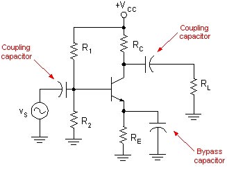
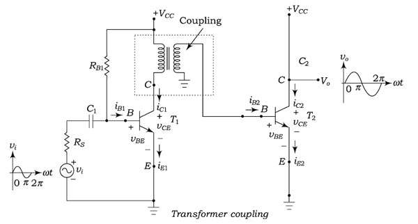
Function of the coupling capacitor In analog circuits, a coupling capacitor is used to connect two circuits such that only the AC signal from the first circuit can pass through to the next while DC is blocked. This technique helps to isolate the DC bias settings of the two coupled circuits. Capacitive coupling is also known as AC coupling and the capacitor used for the purpose is also known as a DC-blocking capacitor. Transformer coupling The Transformer coupling is shown in Fig and is mostly employed for impedance matching. In general. the last stage of the multistage amplifier is the power stage. This stage delivers the maximum power to the load e.g. a loudspeaker. For maximum power transfer, the impedance of the power source must be equal to that of the load. In this scheme, the primary winding of the transformer is used as a collector load and the secondary winding of transformer transmits the ac output voltage signal directly to the base of the next-stage amplifier. Hence there is no requirement of coupling capacitors. Moreover, the secondary winding also provides a base return path, and there is no need for base resistance. Amplifiers using this coupling are called transformer-coupled.
In most of the practical case, you will not see the single amplifier. Rather than you will see a series of the cascaded amplifier. The term cascaded means connected in series. Coupling capacitors are commonly used to connect one amplifier stage to the another.
Ques.22. Which factor influences the critical density of the superconductor?
- Magnetic field strength
- Temperature
- Electric field
- Both 1 & 2✓
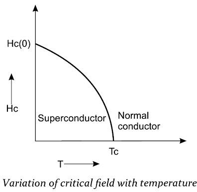
Superconductivity is a phenomenon in which certain metals, alloys, and ceramics conduct electricity without resistance when it is cooled below a certain temperature called the critical temperature. A superconductor is a material that loses all its resistance (offers zero resistance) to the flow of electric current when it is cooled below a certain temperature called the critical temperature or transition temperature TC. Examples: Mercury (Hg), Zinc (Zn), Vanadium (V), Tin (Sn) and Niobium (Nb). Properties of Superconductors Few important properties of superconductors are explained in brief in this section. (i) Critical temperature TC (Transition Temperature) The electrical resistance of the superconducting materials becomes zero below the transition temperature (Tc). This property is called the defining property of superconductors. The figure shows the variation of electrical resistance with respect to the temperature for the normal conductor and a superconductor. From the figure, it is noted that the resistance falls to zero at the transition temperature. Note:- Good electrical conductors such as silver (Ag), Gold (Au) and copper (Cu) are not good superconductors because the resistivity of these conductors at low temperatures is limited to the low resistivity. Similarly, good superconducting materials like Zn and Pb are not good electrical conductors. (ii) Magnetic field effect If a sufficiently strong magnetic field is applied to a superconductor at any temperature below its critical temperature TC, the superconductor is found to undergo a transition from the superconducting state to the normal state. This minimum magnetic field required to destroy the superconducting state is called the critical magnetic field HC. (iii) Electrical resistance:- The electrical resistance of a superconducting material is very low and is of the order of 10–7 Ωm. (iv) Effect of impurities:- When impurities are added to superconducting elements, the superconducting property is not lost, but the TC value is lowered. (v)Critical current density JC and critical current IC The critical current density is another important characteristic feature of the superconducting state. When the current density through a superconducting sample exceeds a critical value JC. the superconducting state is found to disappear in the sample. This happens because, the current through the superconductor itself generates a magnetic field, and at a sufficiently high current density the magnetic field will start exceeding the critical magnetic field HC thereby making the superconducting state to disappear in the material. Hence, the critical current density can be defined as the maximum current that can be permitted in a superconducting material without destroying its superconductivity state. The critical current density is a function of temperature, i.e., colder the temperature for a superconductor the more is the current it can carry. (v) Effect of pressure and stress:- Certain materials are found to exhibit the superconductivity phenomena on increasing the pressure over them. For example, cesium is found to exhibit superconductivity phenomena at TC = 1.5 K on applying a pressure of 110 Kbar. In superconductors, the increase in stress results in an increase of the TC value. (vi) Isotope effects:- The critical or transition temperature TC value of a superconductor is found to vary with its isotopic mass. This variation in TC with its isotopic mass is called the isotopic effect. The transition temperature is inversely proportional to the square root of the isotopic mass of a single superconductor.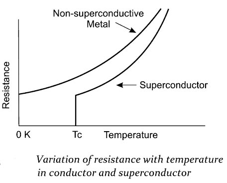
Ques.23. Which among the characteristics of the crystal diode is used for rectification?
- Opposite
- Can’t be determined
- Forward or reversed
- Forward✓
A PN junction is known as a semiconductor diode or crystal diode. A PN-junction diode is formed when a p-type semiconductor is fused to an n-type semiconductor creating a potential barrier voltage across the diode junction. Forward Biasing: If the positive terminal of an external battery is connected to p-type and its negative terminal to n-type of PN junction then such a biasing is called forward biasing. Forward biasing reduces potential barriers and hence, depletion layer width decreases. The current is due to majority carries. Current is quite large when applied, with forward voltage. In forward biasing conditions, the PN junction acts as a Closed switch. Crystal Diode as a Rectifier A crystal diode converts a.c. into d.c. and thus acts as a rectifier. Fig. shows the rectifying action of a crystal diode. During the positive half-cycle of a.c. input, the diode is forward biased and conducts current. During the negative half cycle, the diode is reverse biased and conducts no current. The result is that output consists of positive half-cycles of input a.c. voltage while the negative half-cycles are suppressed. It is interesting to see that the behavior of the diode is like a switch. When the diode is forward biased, it behaves like a closed switch and connects the a.c. supply to the load RL. However, when the diode is reverse biased, it behaves like an open switch and disconnects the a.c. supply from the load RL. This switching action of the diode permits only the positive half-cycles of input a.c. voltage to appear across RL.
Ques.24. Which among the following statements are true with respect to semiconductor breakdown?
- Both the zener breakdown occurs in the junction which is lightly doped and the avalanche breakdown occurs in the junction, which is heavily doped
- The Zener breakdown occur which are heavily doped
- The avalanche breakdown occurs which are heavily doped✓
- None of these
Zener diodes are similar to conventional diodes when they are forward biased When they are reverse biased, no conduction takes place until a specific value of reverse breakdown voltage (or “zoner” voltage) is reached. The Zener is designed so that it will operate in the reverse breakdown region of its characteristics curve. A properly doped junction diode that has sharp reverse breakdown voltage is called a Zener diode. The reverse breakdown of Zener voltage or avalanche breakdown depends upon the amount of doping. If the diode is heavily doped depletion layer will be thin and consequently, the breakdown of the junction will occur at a lower reverse voltage. On the other hand, a lightly doped diode has a higher breakdown voltage. When used as a voltage regulator the zoner diode is reverse biased so that it will operate in the breakdown region. In this region, changes in current through the diode have little effect on the voltage across it. The constant-voltage characteristic of a Zener diode makes it desirable for use as a regulating device. From the VI Characteristics of Zener diode, we can see that the Zener diode has a region in its reverse bias characteristics of almost a constant voltage regardless of the current flowing through the diode This voltage across the diode called Zener voltage VZ remains nearly constant even with changes in current through the diode caused by variations in the supply voltage or load. This ability of the diode to regulate the source voltage can be best utilized in stabilizing a voltage source against supply or load variations. The diode will continue to regulate until the diode current falls below the lZmin ) value, a minimum value that keeps the diode in the reverse breakdown region.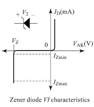
Ques.25. Which law states that an E.M.F is induced in a conductor whenever it cuts flux?
- Gauss’s Law
- Lenz’s Law of electromagnetic induction
- Faraday’s law of electromagnetic induction✓
- Lorentz’s force law
Faraday’s law of electromagnetic induction describes the relationship between the magnetic field and an electric circuit. Faraday gave two laws of electromagnetic induction. 1st law: Whenever the amount of magnetic flux linked with a coil changes, an e.m.f. is induced in the circuit. The e.m.f. lasts so long as the change in magnetic flux continues. Alternatively, it can be stated as: Whenever a conductor (circuit) cuts across the magnetic lines of force, an emf is induced in it. 2nd law: The magnitude of e.m f. induced in a circuit is directly proportional to the rate of change of magnetic flux linked with the circuit.
Ques.26. Which charging method is preferred to avoid sulfation of batteries?
- Both Initial charging & trickle charging
- Quick Charging
- Trickle charging✓
- Initial charging
Sulfation:- “A lead-acid battery can be charged and recharged only a finite number of times because the use of the battery causes crystalline lead sulfate to be deposited and accumulate on the surface of the positive and negative electrodes of the battery. It occurs when batteries are subjected to prolonged undercharge conditions. During normal use, soft sulfate crystals form and dissipate as part of the normal charge and discharge cycle. During periods of prolonged undercharge, the sulfate converts to hard crystals and deposits on the negative plates i.e Lead. With time the crystals grow in size and become hard, covering the lead plates completely. This coverage deteriorates the overall efficiency and powers storage capability of the battery. Sulfation also increases the internal resistance of a battery. This means a higher charging voltage is needed to regenerate active plate material when charging. Trickel Charging:- Trickle charging means charging a fully charged battery by passing a small current at a rate equal to its self-discharge rate, thus enabling the battery to remain at its fully charged level. Due to leakage action and other open-circuit losses, the battery deteriorates even when idle or on open-circuit. Hence, to keep it fresh, the battery is kept on a trickle charge. The rate of trickle charge is small and is just sufficient to balance the open-circuit losses. Trickel charging is the best way to prevent sulfation because it keeps a lead-acid battery in a fully charged state hence lead sulfate does not form.
Ques.27. Which law is the consequences of the law of conservation of energy?
- Lenz’s law✓
- Moore’s law
- Faraday’s law
- Kepler’s law
Lenz’s law provides a way to determine the polarity of an induced emf. As per Faraday’s Law of electromagnetic induction, a current is induced in a conducting loop by the changing magnetic flux. This induced current itself produces a magnetic field and hence a magnetic flux. This magnetic flux may have the same sign as the original magnetic flux or may have the opposite sign. It strengthens the original magnetic flux if it has the same sign or weakens it if opposite sign. Lenz Law states that “ if there is changing magnetic flux through a loop, then an EMF is “induced” in the loop such that the resulting induced current opposes the change..” In other words, Every effect of induction acts in opposition to the cause that produces it. Here the effect is induced current and the cause is changing magnetic flux. That is, the induced current tends to keep the original magnetic flux through the loop from changing. We shall show that this law is a consequence of the law of conservation of energy. To understand Lenz’s law, consider the example of a bar moving to the right on two parallel rails in the presence of a uniform magnetic field (the external magnetic field, Fig. As the bar moves to the right, the magnetic flux through the area enclosed by the circuit increases with time because of the area increases. Lenz’s law states that the induced current must be directed so that the magnetic field it produces opposes the change in the external magnetic flux. Because the magnetic flux due to an external field directed into the page is increasing, the induced current—if it is to oppose this change—must produce a field directed out of the page. Hence, the induced current must be directed counterclockwise when the bar moves to the right. (Use the right-hand rule to verify this direction.) If the bar is moving to the left as in Figure b, the external magnetic flux through the area enclosed by the loop decreases with time. Because the field is directed into the page, the direction of the induced current must be clockwise if it is to produce a field that also is directed into the page. In either case, the induced current attempts to maintain the original flux through the area enclosed by the closed loop. Let’s examine this situation using energy considerations. Suppose the bar is given a slight push to the right. In the preceding analysis, we found that this motion sets up a counterclockwise current in the loop. What happens if we assume the current is clockwise such that the direction of the magnetic force exerted on the bar is to the right? This force would accelerate the rod and increase its velocity, which in turn would cause the area enclosed by the loop to increase more rapidly. The result would be an increase in the induced current, which would cause an increase in the force, which would produce an increase in the current, and so on. In effect, the system would acquire energy with no input of energy. This behavior is clearly inconsistent with all experiences and violates the law of conservation of energy. Therefore, the current must be counterclockwise. Hence Lenz’s Law ensures that, if the electrical energy gained is one unit then the mechanical energy lost is also one unit so that the net energy gain of the wire is zero. Energy is conserved.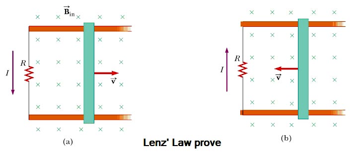
Ques.28. Which one are disadvantages of impedance matching?
- Give low power output
- Give distorted output✓
- Required a transformer
- Generates electrical power
Impedance transformation or matching is an essential part of an amplifier design. Impedance matching is important to achieve optimum noise figure, gain, power, and PAE performance over the required bandwidth by efficiently transferring the signal from a generator to a device, from a device to a load, or between devices. There are a variety of matching networks that can be used for this purpose. The important factors to be considered in the selection of matching networks are (a) bandwidth, (b) frequency response, (c) complexity, and (d) ease of implementation. In order to transfer maximum power to the load, the load impedance must equal the source impedance. In audio power stages which are used to drive a speaker, the output impedance of the transistor is considered to be the source impedance, The load impedance is that of the speaker, which is usually from 4 to 16 ohms. If this load was connected directly to the collector or plate of a power amplifier having a relatively large a.c. output impedance, the transfer of power to the load would be small. Therefore, a method of improving the power transfer to the load must be used. This is the purpose of the IMPEDANCE MATCHING TRANSFORMER. The transformer will match the impedance of the load to the impedance of the source. While perfect impedance matching will not be achieved and the theoretical 50% efficiency cannot be obtained, it is, nevertheless, far superior to connecting the low impedance speaker directly to the amplifying device. One of the disadvantages of using a single-ended power amplifier with transformer coupling is the possibility of core saturation. A direct current is flowing through the primary of the transformer at all times and tends to permanently magnetize the core material of the transformer. If this is allowed to occur, the inductive reactance of the transformer will be reduced which may cause distortion in the form of a losss of gain at low frequencies. Impedance matching is very important for large-signal amplifier and harmonic distortion also occur in large-signal amplifier. Harmonic distortion: This type of distortion occurs when the output contains new frequency components that are not present in the input signal. These new frequencies are the harmonics of the frequencies present in the input. Harmonic distortion in an amplifier occurs because of the non-linearity in the dynamic transfer characteristics curve. Hence this distortion is also called non-linear distortion. In case of voltage amplifier, where small signals are handled, no harmonic distortion occurs. However, in power amplifier due to the large input signal the change in the output current is no longer proportional to the change in input voltage. This type of distortion is also called as amplitude distortion.
Ques.29. Which is to be considered as the most important characteristics of the power amplifier?
- Biasing the circuit
- Collector efficiency✓
- To keep the transformer cool
- None of these
Amplifier:- Any device that increases the magnitude of an applied signal. It receives an input signal(voltage, Current, Power) and delivers a larger output signal that in addition to its increased amplitude, is a replica of the input signal. A power amplifier is an electronic amplifier designed to increase the magnitude of power of a given input signal. The efficiency, along with the linearity, is one of the most critical parameters of power amplifiers. Four efficiency types are often considered. Collector efficiency (ηc) is the ratio of the RF output power (Pout) and the DC input power (PDCin) ηc = Pout ⁄ PDCin Power added efficiency (ηPAE). It considers the RF power increment introduced by each amplification stage. It is obtained by subtracting the RF input power (PRFin) to the RF output power (Pout). In high gain amplifiers, this parameter will practically coincide with the collector efficiency. ηPAE = (Pout − PRFin) ⁄ PDCin Total efficiency (ηT). It is defined as the ratio between the RF power (Pout.) and the input power including the RF excitation (PRFEX). ηT = Pout ⁄ (PDCin + PRFEX) Instantaneous efficiency:- The performance of any previous efficiency rate for a given input signal in the time domain is known as the instantaneous efficiency. Therefore the mean efficiency (ηavg) is defined as the ratio between the output average power (PRFmean) and the DC input power (PDCin). ηavg = PRFmean ⁄ PDCin
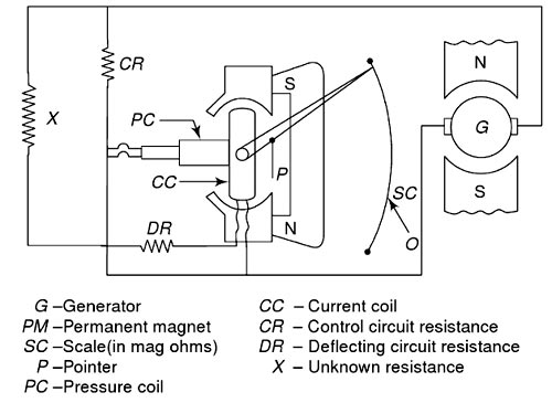
Ques 30. Which part/phenomenon controls the controlling torque in megger?
- Earthing
- Leakage
- Spring
- Coil✓
Insulation testing megger is a portable instrument used for testing the insulation resistance of a circuit, and for measuring the resistance of the order of megaohms in which the measured value of resistance is directly indicated on a scale. Principle: The instrument works on the principle of ratiometer/ohmmeter. The required deflecting torque is produced by both the system voltage and the current Due to interaction between the magnetic fields produced by the voltage and the current, the deflecting torque is produced. The required coils are so positioned that the deflecting torque is proportional to the ratio, VI. It consists of a permanent magnet that provides the field for both the generator G and ohmmeter. One of the moving coils is called the current coil. There are two coils rigidly fixed perpendicular to the current coil and are called voltage coils. The outer voltage coil is called the control coil while the inner voltage coil is called a compensating coil. The torque produced by the current coil opposes the torque produced by the voltage coils. Operation Resistance to be measured is connected across the test terminals, i.e. connected in series with the deflecting coil and across the generator. When currents are supplied to the coils, then they have torques in opposite directions. If the resistance to be measured is high, no current will flow through the deflecting coil. The controlling coil will, therefore, set itself perpendicular to the magnetic axis and hence, sets the pointer at infinity. If the resistance to be measured is small, a high current flows through the deflecting coil and the resulting torques set the pointer to zero. For intermediate values of resistance, depending upon the torque production, the pointer is set at a point between zero and infinity. The hand-driven generator is of permanent magnet type and it is designed to generate from SOO to 2500 volts. Since the Megger’ don’t use the controlling spring. When not in use the pointer can assume any position on the scale.