
A device that does not exhibit negative resistance characteristics is
Right Answer is:
FET
SOLUTION
Field Effect Transistor
A field-effect transistor is a three-terminal semiconductor device in which current conduction is by one type of carrier i.e. electrons or holes. The conduction of current either by electrons or holes in occurred by controlling an electric field between the gate electrode and the conducting channel of the device. It has high impedance and low noise levels.
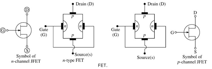
One p-type or n-type silicon bar has two pa junctions at the sides which constitute a FET as shown in Figure 18.1. The bar forms the conducting channel for the charge carriers.
An n-channel FET consists of an n-type semiconductor bar. Two ohmic contacts are made on two ends. One end is called Drain and the other one is known as Source.
Source: The source S is the terminal through which the majority of carriers enter the bar.
Drain: The Drain D is the terminal through which the majority of carriers leave the box.
Gate: On both sides of the semiconductor bar, an impurity region (heavily doped pa region) is formed. These impurity regions are internally connected and a single terminal is taken out which is called gate G.
If a p-type semiconductor bar is used and the two impurity regions are heavily doped n+ regions (Figure 18.1b), the device is referred to as p-channel FET.
There are two types of Field Effect Transistors:
- Junction Field Effect Transistor (JFET)
- Insulated Gate FET (IGFET) or Metal Oxide Semiconductor FET (MOSFET).
Depending on the type of semiconductor bar used in construction, JFET may further be classified as n-channel FET or p-channel FET.
Current is made to flow along the length of JFET semiconductor bar when a voltage is applied between drain and source. The region between the source and drain, sandwiched between the two impurity regions is called the channel, and the majority carrier moves from source to drain through this channel.
The principle of working of these two types of the transistor is similar, the only difference being that in n-channel JFET the current is carried by electrons while is p-channel JFET, it is carried by holes. In the absence of an applied voltage, JFET has gate channel junctions under no bias condition. The result is a deflection region at the junction, as shown in Figure. This represents the same deflection region of a diode under no bias condition. The deflection region in that region does not have any free carriers and therefore is unable to support conduction through the region.
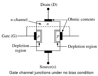
In JFET, the p-n junction between gate and source is always kept in reverse biased conditions. Since the current in a reverse-biased p-n junction is extremely small, practically zero, the gate current in JFET is often neglected and assumed to be zero.
Characteristics of FET
- FET has lower switching losses but its ON-state resistance and conduction losses are more. As a result, for high-frequency applications, power FET is the obvious choice.
- FET is a voltage-controlled device.
- FET has a positive temperature coefficient of resistance which makes the parallel operation of MOSFETs easy. If a MOSFET shares an increased current initially, it heats up faster, its resistance rises and this increased resistance causes the current to shift to other devices connected in parallel.
- In FETs, the secondary breakdown does not occur because it has a positive temperature coefficient. On the other hand, since BJT has a negative temperature coefficient, a secondary breakdown occurs. In BJT, with the decrease in resistance, the current increases. This increased current over the same area results in hot spots and breakdown of the BJT.
- FETs, in higher voltage ratings, have more conduction losses.