The Bohr’s Atomic model explains a simpler understanding on how the structure of neutrons, electrons and protons are constructed. The model is needed to analyze how each of the semiconductor materials Germanium, Silicon and Gallium arsenide are made up of.
In the diagrams below, valence electrons are moving along the Nucleus and they move along the shell regions. Nucleus is the center of an atom.
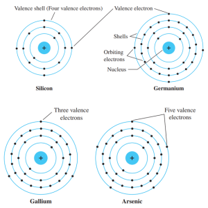
Source: Robert Boylestad, Electronic Devices
In the figures above, Silicon has 14 electrons, Germanium 32 electrons, Gallium 31 electrons and Arsenic 33 electrons.
Si and Ge has 4 valence electrons while Gallium 3 and Arsenic has 5 valence electrons.
3- Trivalent Valence Electrons
4- Tetravalent Valence Electrons
5- Pentavalent Valence Electrons
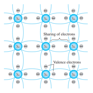
Below is an example of Silicon atom sharing their electrons and they form what we know as covalent bonding.
Each Silicon Atom shares 1 valence electron to adjacent Si Atoms. If the valence electrons receive sufficient kinetic energy, it could dislodge from its location. These dislodge or “free” electron can move freely later if voltage or potential difference is applied to it. At room temperature there are approximately 1.5 x10x10 free carriers in 1 cm 3 of intrinsic silicon material.
An intrinsic material is referred also as low impurity material.
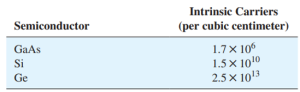
Below is the tabulation of free “intrinsic carrier” on a certain material. Germanium has the highest number. Certain applications especially in high radio frequency requires high numbers of intrinsic carriers.
A semiconductor material is has a negative temperature coefficient, meaning it becomes more conductive at higher temperature as oppose to a conductor which has positive temperature coefficient. A conductor resistivity increases when temperature rises.