
1. The major source of the interference with the desired signal in an electronic system is called
A. Error signal
B. Interference signal
C. Noise signal
D. Faulty signal
2. Identify the external noise sources
A. Switching of rotating machinery
B. Control circuits
C. Ignition system
D. All of the mentioned
3. Which among the following is not a source of internal noise?
A. AC random voltages generated within conductors
B. Lightning
C. Switching of circuits
D. None of the mentioned
4. The type of noise phenomena that increases with an increase in temperature is
A. 1/f noise
B. Schottky noise
C. Thermal noise
D. None of the mentioned
5. The factors that determine the amount of noise induced is
A. Type of coupling between two circuits
B. Rate of change of current per unit time
C. Speed of operation of the circuit
D. All of the mentioned
6. Which type of noise is produced when the op-amp has wider bandwidth?
A. 1/f noise
B. Schottky noise
C. Thermal noise
D. Radiant noise
7. Mention a scheme to reduce the effect of electrical noise on ICs?
A. Isolating ICs on different boards
B. Add a filter near ICs
C. Physical shielding of ICs
D. Use of compensating networks near ICs
8. Internal noise generation can be reduced by keeping
A. None of the mentioned
B. Input lead length short
C. Both input and output lead length short
D. Output lead length short
9. How to choose an IC for a high electrical noise environment?
A. Low degree of noise immunity
B. High degree of noise immunity
C. Low degree of noise reduction
D. High degree of noise reduction
10. Which among the following has the best immunity to induced noise?
A. Non-inverting amplifier
B. Inverting amplifier
C. Differential amplifier
D. Voltage follower
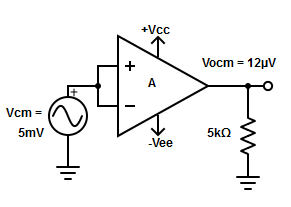
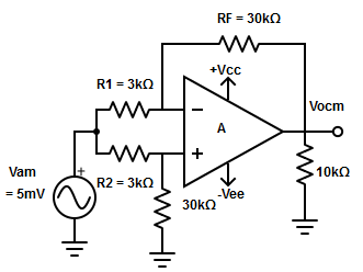
11. Find the output voltage for a differential amplifier, Where Vin->Induced input noise.
A. VO= -[(RF/R1)×Vd]+Vno
B. VO= -(RF/R1)×(Vd/Vno)
C. VO= -[(RF/R1)×Vd]-Vno
D. VO= -[(RF/R1)×Vd]×Vno
12. When does the op-amp said to operate in a common-mode configuration?
A. When the input voltage is equal
B. When the input voltage is equal to the output voltage
C. When the same voltage is applied to both input terminals of an op-amp
D. When different voltage is applied to both input and terminal of an op-amp
13. Common mode voltage gain of an op-amp is generally
A. >1
B. =1
C. <1
D. None of the mentioned
14. Define the common-mode rejection ratio (CMRR) of op-amp?
A. CMRR=AD/ACM
B. CMRR=ACM/ AD
C. CMRR=VOCM/ACM
D. CMRR=AD*ACM
15. Find the correct equation for common-mode rejection ratio
A. CMRR = 20log(AD/ ACM)
B. CMRR = 20log(Vio/ VCM)
C. CMRR = (AD* VCM)/ VOCM
D. All of the mentioned
16. When an op-amp exhibits poor common-mode rejection?
A. Small common-mode output voltage
B. Large common-mode output voltage
C. Negligible common-mode output voltage
D. None of the mentioned
17. Higher value of the common-mode rejection ratio can be reached
A. By reducing the common-mode voltage
B. By decreasing the differential gain
C. By reducing the common-mode input voltage
D. All of the mentioned
18. Variation in the operating frequency of op-amp causes
A. Variation in gain amplifier
B. Variation in gain phase angle
C. Variation in gain amplitude and its phase angle
D. None of the mentioned
19. A graph of the magnitude of the gain versus frequency is called
A. Break frequency
B. Frequency response plot
C. Frequency stability plot
D. Transient response plot
20. In the frequency response plot, the frequency is expressed in
A. Anti-logarithmic scale
B. Logarithmic scale
C. Linear scale
D. Exponential scale
21. Why the gain magnitude in the frequency response plot is expressed in decibels (dB.
A. To obtain gain > 105
B. To obtain gain < 105
C. To obtain gain = 0
D. To obtain gain = ∞
22. Which technique is used to determine the stability of op-amp?
A. Frequency response plot
B. Transient response plot
C. Bode plot
D. All of the mentioned
23. How many types of plots can be obtained in the AC analysis of the network using the Bode plot?
A. Five
B. Four
C. Three
24. What happens when the operating frequency of op-amp increases?
A. Gain of the amplifier decrease
B. Phase shift between output and input signal decrease
C. Gain and phase shift of amplifier decreases
D. None of the mentioned
25. Which of the following causes change in gain and phase shift?
A. Internally integrated Resistor
B. Internally integrated inductors
C. Internally integrated Capacitor
D. All of the mentioned
26. Which plot is not provided by the manufacturers?
A. Magnitude plot
B. Phase angle plot
C. Frequency response plot
D. None of the mentioned