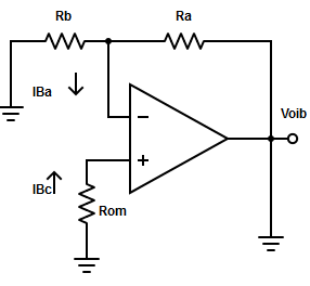
41. Find out the input offset current from the circuit
A. Iio = |IBA*IBC|
B. Iio = |IBA+ IBC|
C. Iio = |IBA/ IBC|
D. Iio = |IBA– IBC|
Answer: D
The input offset current from the circuit is Iio = |IBA– IBC|.
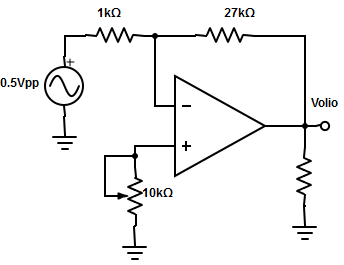
42. Determine the maximum output offset voltage caused by input offset current
A. 5.4mv
B. 7.3mv
C. 6.9mv
D. 8.1mv
Answer: A
For a 741 op-amp
Iio = 200nA(Maximum).
VOIio = RF*Iio
= 27kΩ*200nA =5.4mv.
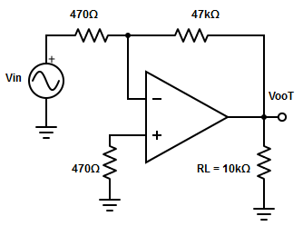
43. Find the total output offset voltage of non-inverting op-amp?
A. VooT = {[1+(RF/R1)]*Vio} + RF*Iio
B. VooT = -[(RF/R1)*Vio] + RF*Iio
C. VooT = -[(RF/R1)*Vio] + Iio
D. None of the mentioned
Answer: B
The gain of the inverting amplifier
A=-(RF/R1).
Therefore, the total output offset voltage is given as
VooT = -[(RF/R1)*Vio] + RF*Iio.
44. Analyse the circuit and determine the value of total output offset voltage?
The op-amp is the MC1536 with the following specifications:
Vio = 7.5mv, Iio = 5nA, IB =250nA.
A. 0.12v
B. 1.4v
C. 0.76v
D. 8.5v
Answer:c
The total output offset voltage due to input offset voltage,
VooT = -[(RF/R1)*Vio] + RF*Iio
VooT = [1+(47kΩ/470Ω)]*7.5mv+(47kΩ*50nA.
= 0.7598 ≅ 0.76v.
45. Which factor affects the input offset voltage, bias current, and input offset current in an op-amp?
A. Change in temperature
B. Change in supply voltage
C. Change in time
D. All of the mentioned
Answer: D
The factor that affects the input offset voltage, bias current, and input offset current in an op-amp are
Change in temperature
Change in supply voltage
Change in time
Any change in the mentioned parameters affects the values of input offset voltage, bias current and input offset current from remaining constant.
46. Thermal voltage drift is defined as
A. △Vio/△T
B. △VF/△T
C. △Iio/△T
D. △IB/△T
Answer: A
The average rate of change of input offset voltage per unit change in temperature is called thermal voltage drift, i.e.
△Vio/△T.
47. A completely compensated inverting amplifier is nulled at room temperature 25oC, determine the temperature at which the total output offset voltage will be zero?
A. 50oC
B. 25oC
C. 75oC
D. 125oC
Answer: B
When an amplifier is nulled at room temperature, the effect of input offset voltage and current is reduced to zero.
Change in the total output offset voltage occurs only if there is any change in the value of Vio and Iio. Therefore, the total output offset voltage will be zero at room temperature i.e at 25°C.
48. How the effect of voltage and current drift on the performance of an amplifier is determined?
A. △VooT/△T = {[1-RF/R1)]×(△Vio/△T)} + RF×(△Iio/△t)
B. △VooT/△T = {(-RF/R1)×(△Vio/△T)} + RF×(△Iio/△t)
C. △VooT/△T = {[1+(RF/R1)]×(△Vio/△T)} + RF×(△Iio/△t)
D. None of the mentioned
Answer: C
As the amplifier is used in inverting configuration, the effect of voltage and current drift is given as, the average change in total output offset voltage per unit change in temperature.
49. The error voltage in a compensating inverting amplifier is obtained by
A. Multiplying △T to total output offset voltage
B. Multiplying △T to input offset voltage
C. Multiplying △T to input offset current
D. All of the mentioned
Answer: A
The maximum possible change in the total output offset voltage △VooT results from a change in temperature △t.
Therefore, the error voltage is obtained by multiplying △T by the average total output offset voltage.
Ev =( △VooT/△T)×△T = [1+(RF/R1)]×(△Vio/△T)×△T + RF×(△Iio/△T)×△T.
50. A 7.5kΩ internal resistor and a 12kΩ feedback resistor are connected to an inverting amplifier. Find the error voltage, if the output voltage is 3.99mv for input of 1.33mv.
A. ±0.6v
B. ±0.6mv
C. ± 60mv
D. ±6mv
Answer: D
The output voltage of inverting amplifier is
Vo= -(RF/R1)×Vin±Ev
=> Ev= ± Vo+(RF/R1)×Vin
= 3.99mv+(12kΩ/7.5kΩ)×1.33mv
= ±6.118 ≅ ±6mv.
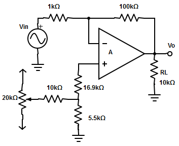
51. Consider the amplifier is nulled at 27oC. Calculate the output voltage , if the input voltage is 6.21mv dc at 50oC. Assume LM307 op-amp with specification:
△Vio/△T=30µV/oC ; △Iio/△T = 300pA/oC; VS =±15v.
A. +0.53v or -0.68v
B. +0.52v or -0.78v
C. +0.54v or -0.90v
D. +0.51v or -0.86v
For an input voltage of 6.21mv dc, the output voltage,
Vo=-(RF/R1)×Vin±Ev
= -(100kΩ/1kΩ) × 6.21mv ± 70.4mv
= +0.69v or -0.55v.
52. Which factor affects the power supply voltages in the amplifier?
A. Poor regulation and filtering
B. Resistive network connected to an amplifier
C. Change in temperature
D. All of the mentioned
Answer: A
A poorly regulated power supply gives different values depending on the size & type of load connected to it and a poorly filtered power supply has a ripple voltage riding on some specific dc level.
53. Change in the input bias current does not affect?
A. Input offset voltage
B. Output offset voltage
C. Input offset current
D. Output offset current
Answer: C
Even though the input bias currents change due to the change in supply voltages, the input offset current remain relatively constant because it is the absolute value of the difference between two input bias currents.
54. A supply voltage rejection ratio of 15µv/v is given for an op-amp. Find its equivalent value in decibels
A. 74db
B. 77dB
C. 76.48dB
D. 76dB
Answer: C
Supply voltage rejection ratio, SVRR in dB
= 20log(1/SVRR) =20log[1/(△Vio/△V)]
= 20log(1/150µV/V)
=20log(106/150)
=20log(6666.67) = 76.48dB.
55. When does the op-amp perform better?
A. Low value of SVRR in µV/V
B. High value if SVRR in µV/V
C. Low value of SVRR in dB
D. High value of SVRR in dB
Answer: A
The total value of SVRR in µV/V should be zero. The lower the value of SVRR in µV/V, the better will be the op-amp performance.
56. Write the equation for change in the output offset voltage?
A. △Voo = [-RF/R1)]× [△Vio/△V] ×△V
B. △Voo = [1+(RF/R1)]× [△Vio/△V] ×△V
C. △Voo = [1+(RF/R1)]× [△Vio/△V].
D. None of the mentioned
Answer: B
The change in the input offset voltage is given as
△Voo =[1+(RF/R1)]× [△Vio/△V] × △V
Where
△V = Change in supply voltage +Vcc & -Vee,
△Vio/△V = Supply voltage rejection ratio (µV/V) and
[1+(RF/R1)] = Gain of the differential amplifier.
57. A LM307 amplifier has an SVRR of 92dB, express it in terms of microvolts per volts?
A. 65µV/V
B. 37.98µV/V
C. 25.12µV/V
D. 101.4µV/V
Answer: C
20log(1/SVRR) = 92dB
=> log(1/SVRR) = 92/20
=> 1/SVRR= 104.6
=> SVRR = 1/104.6 = 25.12µV/V.
58. Which value remains the same regardless of whether it is computed from the change in low dc supply or change in +Vcc or -Vee?
A. △V
B. △Vio
C. △Voo
D. None of the mentioned
Answer: D
△V value is the same regardless of whether it is computed from the change in low dc supply or change in +Vcc or -Vee.
For example, suppose that -Vee remains constant at -10v then the +Vcc has to vary from 8 to 12v as a result of a change in low dc voltage. This means that the change in △V in supply voltage +Vcc is 2v in either direction from 10v.
59. Consider LM307 is initially nulled. Suppose, the op-amp has a poor filter, 20mVrms then ac ripple is measured across the terminals. If Vin=0v, determine the change in output offset voltage caused by the change in supply voltage?
A. 81µVrms
B. 8.1µVrms
C. 0.81µVrms
D. 810µVrms
Answer: B
The SVRR = 15.85µV/V
for LM307 because of poor filtering and △V= 10mVrms.