Semiconductor MCQ
Ques.1. The resistivity of a semiconductor ____________ conductors and insulators
- More than that of
- Lies between that of
- Less than that of
- None of the above
Answer.2. Lies between that of Explanation:- Semiconductors are those materials which have electrical conductivities lying between those of good conductors and insulators. The resistivity of semiconductors varies from 10−5 to 10+4 ohm-meter as compared to the values ranging from 10−7 to 10−6 ohm-meter for conductors and from 107 to 108 ohm-meter for insulators.
Ques.2. A semiconductor is formed by __________ bonds
- Covalent
- Electrovalent
- Co-ordinate
- None of the above
Answer.1. Covalent Explanation:- A semiconductor atom having four valence electrons and four holes require four more electrons so as to make the outermost orbit completely filled (total number must be eight). The atoms in a crystal are arranged so closely that electrons orbit in valence shells of two atoms. Each valence shell electron fills the hole of the neighboring atom as shown in Fig. In the figure, atoms of silicon material have been shown. For ease of understanding, only the outermost orbits of atoms have been shown. Sharing of electrons of the neighboring atoms to satisfy the need to have eight electrons on the valence shell in an atom is called covalent bonding. Thus the covalent bond is formed by sharing of electrons between similar atoms. Because of covalent bonding, i.e., bonding through sharing of electrons, it is seen that the valence shells of all the electrons are full, i.e., all of them have eight electrons in their outermost orbit. At absolute zero temperature, there will be no free electrons in the crystal. However, although the electrons are bound to their atoms due to covalent bonding, a rise in temperature breaks some of the covalent bonding and make some electrons free. A semiconductor material, silicon or germanium where the electrons are bound to their respective atoms and are not free to conduct electric current, are called intrinsic, or pure semiconductors. When the temperature of the crystal is raised, external energy in the form of heat gets applied to the semiconductor material. This heat energy enables the valence electrons to acquire sufficient energy to break away from the atoms and become free electrons. When an electron leaves to become free, it leaves a vacant space called a hole. For every free electron, there will be a corresponding hole produced, which is called an electron-hole pair. A large number of such electron-hole pairs are formed due to rise in temperature of the semiconductor.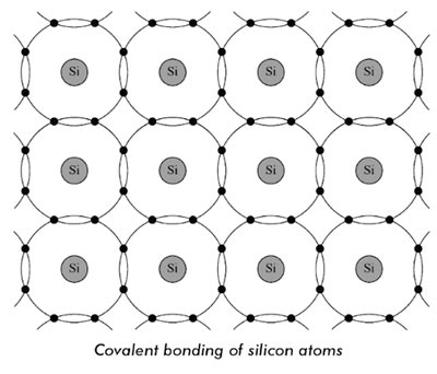
Ques.3. The most commonly used semiconductor is _________
- Germanium
- Carbon
- Sulfur
- Silicon
Answer.4. Silicon Explanation:- Silicon is the most widely used semiconductor material because it has a useful temperature range and is abundant, cheap, and easy to manufacture. Germanium was among the first semiconductor materials to be developed and is less widely used than silicon, but it is useful in very high-speed devices when alloyed with silicon. High-speed semiconductors widely use gallium-arsenide. It is the most commonly used material after silicon; however, it is more expensive and more difficult to manufacture. Silicon carbide has been used to create blue light-emitting diodes (LEDs), and it can withstand high operating temperatures.
Ques.4. In a semiconductor, the energy gap between the valence band and conduction band is about________
- 5 eV
- 10 eV
- 15 eV
- 1 eV
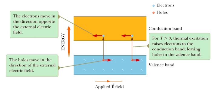
Answer.4. 1eV Explanation:- When atoms form solids, their electron energy states split into many close energy levels that form allowed energy bands. In each energy band, allowed energy levels are very close to each other, and the electron energy can vary continuously. These bands are separated by a forbidden energy gap. The important property of electrons is determined by the rule that is called the Pauli exclusion principle. According to this principle, not more than two electrons with different spins can occupy each energy state. Electrons occupy the lowest energy levels first. In semiconductors and dielectrics, almost all the states in the lowest energy bands are filled by electrons, whereas the energy states in the higher energy bands are, by and large, empty. The lower energy bands with mostly filled energy states are called the valence bands. or The band formed by a series of energy levels containing the valence electrons is known as valence band. The valence band may be partially or completely filled up depending upon the nature of the crystal. The higher energy bands with mostly empty energy states are called conduction bands. The difference between the highest valence band and the lowest conduction band is called the energy band gap or the energy gap. An electron in a valence band needs the exert equal to or higher than the energy gap to experience a transition from the valence to the conduction band. Semiconductors Semiconductors have the same type of band structure as an insulator; but the energy gap is much smaller, on the order of 1 eV. The forbidden energy gap for germanium is 0. 7 em and for silicon 1.1 em The band structure of a semiconductor is shown in Figure. Because the Fermi level is located near the middle of the gap for a semiconductor and Energy gap Eg is small, appreciable numbers of electrons are thermally excited from the valence band to the conduction band. Because of the many empty levels above the thermally filled levels in the conduction band, a small applied potential difference can easily raise the energy of the electrons in the conduction band, resulting in a moderate current. At T = 0 K, all electrons in these materials are in the valence band and no energy is available to excite them across the energy gap. Therefore, semiconductors are poor conductors at very low temperatures. Because the thermal excitation of electrons across the narrow gap is more probable at higher temperatures, the conductivity of semiconductors increases rapidly with temperature, contrasting sharply with the conductivity of metals, which decreases slowly with increasing temperature. Charge carriers in a semiconductor can be negative, positive, or both. When an electron moves from the valence band into the conduction band, it leaves behind a vacant site, called a hole, in the otherwise filled valence band. This hole (electron-deficient site) acts as a charge carrier in the sense that a free electron from a nearby site can transfer into the hole. Whenever an electron does so, it creates a new hole at the site it abandoned. Therefore, the net effect can be viewed as the hole migrating through the material in the direction opposite the direction of electron movement. The hole behaves as if it were a particle with a positive charge +e. Note:- The energy gap of an insulator is 5 eV The energy gap of the conductor is 0 eV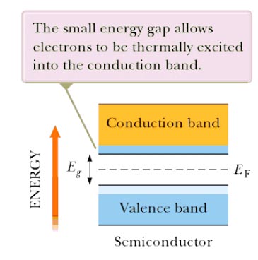
Ques.5. A semiconductor has ____________ temperature coefficient of resistance.
- Negative
- Positive
- Zero
- None of the above
Answer.1. Negative Explanation:- In terms of energy bands, semiconductors can be defined as those materials which have almost an empty conduction band and almost filled valence band with a very narrow energy gap separating the two bands At low temperature, the valence band of a semiconductor is completely filled and the conduction band is completely empty. Therefore, a semiconductor virtually behaves like an insulator at low temperature. However, at room temperature, some electrons cross over to the conduction band giving a little conductivity to the semiconductor. As the temperature is increased more valence electrons cross over to the conduction band and conductivity increases. This shows that electrical conductivity of a semiconductor increases with the increase of temperature, i.e., a semiconductor has a negative temperature coefficient of resistance. Whereas in the case of conductors, when the temperature increases its resistivity increases as electrons collide more frequently with vibrating atoms. This reduces drift speed of electrons (and thus current reduces). Thus conductors have a positive temperature coefficient of resistance.
Ques.6. A semiconductor generally has ____________ valence electrons
- 2
- 3
- 4
- 6
Answer.3. 4
Explanation:-
Semiconductors are neither conductors nor insulators. The commonly used semiconductor elements are silicon, germanium, and gallium arsenide. Silicon is the most widely used semiconductor material. It has 14 protons and 14 electrons in orbits. An isolated silicon atom has four electrons in the valence bond. Germanium has 32 protons, 32 electrons, and 4 valence electrons like silicon.
Ques.7. The resistivity of pure germanium under the standard condition is about
- 6 × 10⁴ Ω cm
- 60 Ω cm
- 3 × 10⁻³ Ω cm
- 6 × 10⁻⁴ Ω cm
Answer.2. 60 Ω cm Explanation:- The ability of a material to conduct current is directly proportional to the number of free electrons in the material. Good conductors, such as silver, copper, and aluminum, have large numbers of free electrons; their resistivities are of the order of a few millionths of an ohm-centimeter. Insulators such as glass, rubber, and mica, which have very few loosely held electrons, have resistivities as high as several million ohm-centimeters. Semiconductor materials lie in the range between these two extremes, as shown in Fig. Pure germanium has a resistivity of 60 Ω cm. Pure silicon has a considerably higher resistivity, in the order of 60,000 Ω cm. As used in semiconductor devices, however, these materials contain carefully controlled amounts of certain impurities, which reduce their resistivity to about 2 Ω cm at room temperature and this resistivity decreases rapidly as the temperature rises.![]()
Ques.8. The resistivity of pure silicon is about___________
- 100 Ω cm
- 60,000 Ω cm
- 3 × 10⁶ Ω cm
- 1.6 × 10⁻⁸ Ω cm
Answer.2. 60,000 Ω cm Explanation:- Semiconductor materials lie in the range between conductor and insulator, as shown in Fig. Pure germanium has a resistivity of 60 Ω cm. Pure silicon has a considerably higher resistivity, in the order of 60,000 Ω cm. As used in semiconductor devices, however, these materials contain carefully controlled amounts of certain impurities, which reduce their resistivity to about 2 Ω cm at room temperature and this resistivity decreases rapidly as the temperature rises.![]()
Ques.9. When a pure semiconductor is heated, it’s resistance_______
- Goes down
- Goes up
- Remains the same
- None of the above
Answer.1. Goes down Explanation:- In a pure semiconductor the four valence electrons of the crystal atom form covalent bonding and at low temperatures, free electrons are not available for conduction of electricity. At 0 K, all valence electrons are strongly bound to their atoms and are actively participating in the covalent bond formation. As a result, no free electrons are available for conduction and it acts as an insulator. At room temperature (T> 0 K), the valence electron acquires a sufficient amount of thermal energy. As a result, breakage of covalent bonds takes place releasing free electrons. These free electrons create a vacancy in its initial position in the crystal. This vacancy is known as a hole and is assumed to carry a positive charge equivalent to the charge of the electron. These free electrons, due to acquiring of sufficient thermal energy, cross the energy gap and enter into the conduction band from the valence band and occupy the energy levels in the conduction band. The electrons leaving the valence band create holes in its place. Thus, the valence band has holes while the conduction band has electrons. The corresponding crystal structure along with the energy band structure is as shown in Fig. Because there are so few electrons that are mobile at room temperature, only a small amount of current will flow through the semiconductor at room temperature.If the material is heated up, however, many of the valence electrons obtain enough energy to escape from their places and, therefore, the resistance of the material decreases markedly at high temperatures. 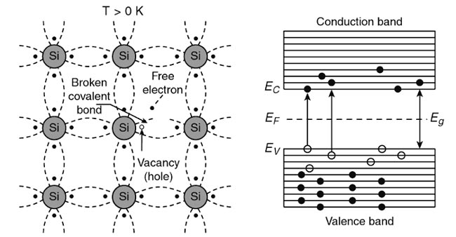
Ques.10. The strength of a semiconductor crystal comes from______
- Forces between nuclei
- Force between protons
- Electrons-Pairs bonds
- None of the above
Answer.3. Electrons-Pairs bonds Explanation:- Crystal. Each atom that is normally bonded with the nearest neighbor atoms results in a special shape called a crystal (Fig). A silicon atom that is a part of a crystal has eight electrons in the valence orbit and four neighbor atoms. Each of the four neighbors shares one electron. Since each shared electron in Fig. is being pulled in opposite directions, it is a kind of a bond between the opposite cores. This type of bond is known as a covalent bond. The covalent bonds hold the tetravalent crystal together, ensuring its stability. A semiconductor atom having four valence electrons and four holes require four more electrons so as to make the outermost orbit completely filled (total number must be eight). The atoms in a crystal are arranged so closely that electrons orbit in valence shells of two atoms. Each valence shell electron fills the hole of the neighboring atom as shown in Fig.![]()


