Ohms Law applies to metal conductors – but only if they are kept at a constant temperature. Then the current in the metal will be proportional to the applied voltage. This means that a graph of current against voltage will be a straight line. But if the current heats a metal conductor it usually becomes more resistive. Current finds it harder to get through as the resistance of the conductor increases. This is what happens in an ordinary filament lamp. The metal filament does obey Ohm’s Law – but we can’t apply it because the temperature is changing from room temperature to a white-hot 2000°C.
Some conductors don’t obey Ohms Law at all. This is especially true of semiconductors Where the number of particles that actually carry the current can change with circumstances. For example, a light-dependent resistor will have more free electrons to carry current when the light on it is brighter. A semiconductor diode is used in electronic circuits because it obeys Ohm’s Law in one direction (more or less) but doesn’t allow any current at all to pass in the opposite direction. The voltage or current do not change with the same magnitude as the change in current or voltage, respectively. So, we can say a diode has a variable resistance. Since a diode has a variable resistance, it is a non-linear device.
Ques.82. In a semiconductor crystal, if the current flows due to breakage of crystal bonds, then the semiconductor is called
Acceptor
Donor
Intrinsic semiconductor
Extrinsic semiconductor
Answer.3. Intrinsic semiconductor
Explanation:-
In the intrinsic semiconductor, some of the covalent bonds break at room temperature, producing free electrons and an equal number of holes. When p.d. is applied across an intrinsic semiconductor, the small current that flows through the material is due to the movement of free electrons and holes.
Ques.83. A P-Type semiconductor is
Uncharged
Positively charged
Negatively charged
None of the above
Answer.1. Uncharged
Explanation:-
Charge on n-type and p-type Semiconductors
In an n-type semiconductor, current conduction is due to an excess of electrons whereas, in a p-type semiconductor, conduction is by holes. We may think that n-type material has a net negative charge and p-type a net positive charge. But this conclusion is wrong. It is true that n-type semiconductor has an excess of electrons but these extra electrons were supplied by the atoms of donor impurity and each atom of donor impurity is electrically neutral. When the impurity atom is added, the term “excess electrons” refers to excess with regard to the number of electrons needed to fill the covalent bonds in the semiconductor crystal. The extra electrons are free electrons and increase the conductivity of the semiconductor. The situation with regard to the p-type semiconductor is also similar. It follows, therefore, that n-type, as well as p-type semiconductor, is electrically neutral.
The n-type semiconductor thus formed remains electrically neutral, i.e., neither positively charged nor negatively charged. This is because the total number of electrons including the free electrons is equal to the total number of protons in the nuclei of the atoms.
Ques.84. The energy gap between conduction band and the valence band of a substance is of the order of 0.07 eV. It is
An insulator
An alloy
A semiconductor
A Conductor
Answer.4. A Conductor
Explanation:-
The energy gap (= 0.07 eV) is so small that valence band virtually touches the conduction band. Therefore, the substance is a conductor.
Ques.85. A semiconductor is cooled from T1K to T2K. Its resistance
Will decrease
Will Increase
Will remain unchanged
Will first increase and then decreased
Answer.1. Will decrease
Explanation:-
A semiconductor has a negative temperature coefficient of resistance i.e. its resistance decreases with the increase in temperature and vice-versa. Therefore, when a semiconductor is cooled, its resistance will increase.
Ques.86. The current in reverse bias in P-N junction diode may be
Between 2A and 5A
Few micros or nanoamperes
Few milliamperes
Between 0.2A and 2A
Answer.2. Few micros or nanoamperes
Explanation:-
Reverse biasing means, applying an external voltage which is opposite in direction to forward bias i.e connecting the positive terminal of the battery to n-side of the diode and negative terminal of the battery to p-side of the diode.
Under reverse bias, the diode does not conduct when the applied voltage is changed. The current remains constant at a negligibly small value (in the range of microamps) for a long range of change in applied voltage.
Ques.87. When reverse biased, a PN junction diode acts as a
An Open circuit
A rectifier
A short circuit
An amplifier
Answer.1. An Open circuit
Explanation:-
A diode is a two-electrode (two-terminal) device that acts as a one-way conductor. The most basic type of diode is the PN-Junction diode. When forward bias PN junction diode conducts. When reverse biased, it effectively blocks the flow of charge (current).
A diode permits current Bow when the voltage on the anode is positive with respect to the voltage on the cathode.
A diode inhibits current flow when the voltage on the anode ~ negative with respect to the voltage on the cathode.
A diode is called forward biased when the anode is positive with respect to the cathode. A forward-biased diode functions like a closed switch permitting current flow.
A diode is called reversed biased when the anode is negative with respect to the cathode. A reversed biased diode functions like an open switch (infinite Resistance) inhibiting current flow.
Based on the characteristics of a switch the following statements can be considered about the ideal diode:
When forward biased enclosed switch):
The diode has no resistance.
The diode does not limit the circuit current
The diode has no voltage drop across its terminals.
When reverse biased (open switch):
The diode has infinite resistance.
The diode does not pass current.
The diode drops the applied voltage across its terminals.
Ques.88. Which one of the following materials is the semiconductor
Chromium
Selenium
Bismuth
Silica
Answer.2. Selenium
Explanation:-
Selenium is produced as a byproduct in the refining of metal sulfide ores. Selenium is a semiconductor and is used in photocells. Applications in electronics, once important, have been mostly replaced with silicon semiconductor devices.
Ques.89.Avalanche breakdown occurs at a reverse bias voltage of
2-4 V
4-6 V
6-8 V
8-10 V
Answer.4. 8-10 V
Explanation:-
Avalanche Breakdown:
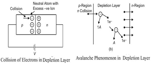
With increasing reverse bias voltage, the electric field across the junction of a p-n diode increases. At a certain reverse bias, the electric field imparts sufficiently high energy to a thermally generated carrier crossing the junction. This carrier, on colliding with a crystal ion on its way, disrupts a covalent bond and produces a new electron-hole pair. These carriers can also gain sufficient energy from the applied field and collide with other crystal ions to generate further electron-hole pairs. The process is cumulative and produces an avalanche of carriers in a very short time. Avalanche breakdown is sometimes called Impact breakdown.
The avalanche breakdown takes place in a junction having a wide depletion layer. With a rise of temperature, the crystal ions vibrate with greater amplitude, increasing the possibility of collisions of the carriers and the crystal ions. The carriers thus have less opportunity to pick up enough energy between collisions to trigger the avalanche process. Consequently, the avalanche breakdown voltage (which is higher than 6 V) increases with a rise of temperature. The reverse bias voltage is applied is relatively higher of the order of 8 – 10 V depending upon doping. Thus the temperature coefiicient of the avalanche breakdown voltage is positive. The change of the breakdown voltage is about 0.1 percent per centigrade degree change of the diode temperature.
Ques.90. Diffusion Capacitance of a PN junction diode ___________ with forward bias.
Increase
Decrease
May increase or decrease
Remain the same
Answer.1. Increase
Explanation:-
The diffusion capacitance occurs due to stored charge of minority electrons and minority holes near the depletion region. Diffusion capacitance is also sometimes referred to as the storage capacitance.
When a P-N junction is forward biased, a capacitance which is much larger than the transition capacitance comes into play. This type of capacitance is called the Diffusion Capacitance. Diffusion capacitance occurs due to stored charge of minority electrons n minority holes near the depletion region. when the width of the depletion region decreases, then diffusion capacitance increases