Ques 21. An iron core chokes coil when connected across 15V supply draws a current of 1.5A. When connected across 230 V, 50Hz supply, it takes 2A current and consumes 60 W. The iron loss will be
- 27.5 W
- 60 W
- 80 W
- 120 W
Wrong Option:- For DC Voltage = 15 V For AC Voltage = 230 V Total loss = Loss in resistance + Iron loss Iron loss = Total Loss – Loss in resistance Pi = P − I2R For DC supply R = 15 ⁄ 1.5 = 10Ω Therefore Iron Loss is equal to Pi = 50 − 1.52 × 10 Pi = 27.5 W
Current = 1.5 A
Current = 2 A
Power = 60 W
Ques 22. The pair of acceptor impurities for the semiconductor material is
- Gallium and Helium
- Arsenic and Antimony
- Gallium and Indium✓
- Arsenic and Argon
Replacing some Si atoms with atoms from Group III (boron, gallium, indium—also known as acceptor impurities), which have three valence electrons, will create a p-type material. Because four valence electrons are required to form and complete all adjacent electron-pair bonds, a hole is created by the missing bond. A hole can be considered a positive charge which can diffuse or drift through a crystal. This becomes important when an external voltage is applied across the semiconductor, creating an electric field inside the semiconductor which then acts on the holes, causing them to move. The resultant current in p-type material is thus primarily by positive charges, which are also referred to as majority carriers. p-type doping is illustrated in Fig. Important Points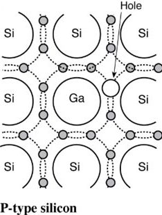
Ques 23. Magnetic locking of the rotor with the stator in case of an induction motor may be reduced by
- Laminating the rotor core
- Equalizer connection
- Skewed Rotor slots✓
- Using Inter-poles
Rotor conductors are skewed because of these two main reasons Cogging:- Skewing the rotor bars prevents the locking thus preventing Cogging. Crawling:– Crawling is a phenomenon where harmonic components introduce oscillations in torque. With the bar skewed, the amount of the bar cutting the field line grows continuously and the next bar starts cutting the field lines as the first finishes. Due to this, we get Uniform Torque.
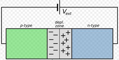
Ques 24. A reverse Biased PN Junction will act as an
- Amplifier
- Open switch✓
- Closed Switch
- Attenuator
Ques 25. In a measuring Instrument, the torque produced by the measurand is called as
- Starting Torque
- Deflecting Torque✓
- Controlling Torque
- Damping Torque
Measurand: The quantity or variable being measured is called measurand. Basically, there are three types of Force or torque that act upon the Measuring Instrument Deflecting Torque: In order to move the pointer from its zero position on the scale deflecting torque is required. The deflecting torque works on the moving system to which the pointer is attached. Obviously, the magnitude of deflecting torque produced is proportional to the magnitude of the quantity being measured, say, the current I flowing through the instrument. A deflecting torque is required to overcome the inertia, damping effect, and controlling effect of the moving system. This deflecting torque can be produced by any of the effects of current (or voltage) such as Controlling Torque: With the help of the deflecting torque, the pointer deflection will take place on the calibrated scale but to stop the pointer at the definite position, controlling torque (Tc.) comes into action. As the deflection of the pointer increases, the controlling torque also increases and stops the pointer at the measured value. Controlling torque is also known as restoring torque i.e., it brings back the pointer to its zero position when deflecting torque is withdrawn. The pointer attains a steady position when controlling torque becomes numerically equal to deflecting torque i.e., Tc = Td Spring control and gravity control are used for controlling torque. Damping Torque: At the final deflected position, when the deflecting and controlling torques are equal, the pointer starts oscillating owing to its inertia and therefore, cannot immediately settle at its final deflected position. If no extra force is provided to dampen these oscillations, the moving system will take considerable time before coming to settle to the final deflected position. This is especially undesirable if the number of readings to be taken is quite large.
Ques 26. A 50 Hz current of zero references has an average value of 45A. Its instantaneous value at an angle of 30° is
- 32 A
- 22.5 A
- 61 A
- 35.33 A✓
The formula of an average value of current is Iavg = 0.637 × Im Where Im = peak or maximum value of current 45 = 0.637 × Im Im = 70.643 A The instantaneous value of the sine wave for any angle of rotation is expressed by the following formula I = Imsinθ Hence the instantaneous value of current for an angle of 30° is I = 70.643 × sin30° I = 35.32
= 70.643 × .5
Ques 27. Select the wrong option related to the statement given below
The main characteristic of the series circuit is that
- Power is additive
- The same current flows through the all parts of the circuit
- Applied voltage equals the sum of the different voltage
- Different resistors have the same voltage drop✓
There are several important characteristics of series circuits. Remember the following basic rules for series circuits: The voltage across a resistor is often called a “voltage drop.” Now suppose two resistors of 10Ω and 20Ω are connected in series and the current in the circuit is 2A. Therefore voltage drop across 10 ohms resistance is V = I x R = 2 x 10 = 20 V Voltage drop across 20 ohm resistor is V = I x R = 2 x 20 = 40 V Hence it is clear that the different resistors have a different voltage drop
Ques 28. An extrinsic semiconductor has
- More number of holes than free electron
- More number free electrons than holes
- Either more holes or more free electrons✓
- Equal number of holes and free electrons
The semiconductor is divided into two types. One is an Intrinsic Semiconductor and the other is an Extrinsic semiconductor. Intrinsic Semiconductors A sample of the semiconductor in its purest form is called an intrinsic semiconductor. The impurity content in the intrinsic semiconductor is very very small, of the order of one part in 100 million parts of the semiconductor. Extrinsic Semiconductor In order to change the properties of intrinsic semiconductors a small amount of some other material is added to it. The process of adding other material to the crystal of intrinsic semiconductors to improve its conductivity is called doping. The impurity added is called dopant. The doped semiconductor material is called extrinsic semiconductors. The doping increases the conductivity of the basic intrinsic semiconductors hence the extrinsic semiconductors are used in practice for the manufacturing of various electronic devices such as diodes, transistors, etc. Depending upon the type of impurities, the two types of extrinsic semiconductors are, N-TYPE Impurity The impurity material having five valence electrons is called the pentavalent atom. When this is added to an intrinsic semiconductor, it is called donor doping as each impurity atom donates one free electron to an intrinsic material. Such an impurity is called donor impurity. Examples of such impurities are arsenic, bismuth, phosphorous, etc. This crests an extrinsic semiconductor with a large number of free electrons called an n-type semiconductor. P-TYPE Impurity Another type of impurity used is the trivalent atom which has only three valence electrons. Such an impurity is called acceptor impurity. When this is added to an intrinsic semiconductor, it crests more holes and is ready to accept an electron hence the doping is called acceptor doping. Examples of such impurities are gallium, indium, and boron. The resulting extrinsic semiconductor with a large number of holes is called a p-type semiconductor. Hence the extrinsic semiconductor may have either a large number of electrons or holes
Ques 29. In the case of three-phase alternating voltages, various voltages are displaced at an angle of
- π/3
- 2π/3✓
- 4π/3
- 3π/2
In electrical engineering, three-phase electric power systems have at least three conductors carrying alternating current voltages that are offset in time by one-third of the period. A three-phase system may be arranged in delta (∆) or star (Y). In a three-phase system, the order in which the voltages attain their maximum positive value is called Phase Sequence. The order in which the phase voltages of a 3-phase system attain their peak or maximum positive values is called the phase sequence of the system. The phase sequence RYB normally means that the red phase is followed by the yellow phase, which is followed by the blue phase. When the voltage of the red phase is at its positive maximum value, the voltage of the Y-phase will be 120° (2π/3) behind its positive maximum value and that of the B-phase 240° behind its positive maximum value as shown in fig. Then Red phase VRN = Vm sinθ If the red phase voltage, VRN is taken as the reference voltage so the voltage in the yellow phase lags VRN by 120°, and the voltage in the blue phase lags VYN also by 120°. But we can also say the blue phase voltage, VBN leads the red phase voltage, VRN by 120°. As the three individual sinusoidal voltages have a fixed relationship between each other of 120o they are said to be “balanced” therefore, is a set of balanced three-phase voltages their phasor sum will always be zero as Va + Vb + Vc = 0
Yellow Phase VYN = Vm sin(θ – 120°)
Blue Phase VBN = Vm sin(θ – 240°)
or VBN = Vm sin (θ + 240°)
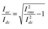
Ques 30. The ripple factor in a full-wave rectifier is
- 1.21
- 0.004
- 0.48✓
- 1.41
Ripple Factor (r): It is the ratio of the root mean square (RMS) value of AC component to the DC component in the output and is given by For full-wave rectifier Irms = Im/√2 Idc =2Im/π Substituting the value in the above expression we get $\begin{array}{l}\gamma = \sqrt {{{\left[ {\dfrac{{{I_m}/\sqrt 2 }}{{2{I_m}/\pi }}} \right]}^2} – 1} \\\\\gamma = \sqrt {\dfrac{{{\pi ^2}}}{8} – 1} \\\\\gamma = 0.48\end{array}$ Note:- The ripple factor of half-wave rectifier is 1.21.