Ques.31. A device, which detects the fault and supplies information to the breaker for circuit interruption is called:
- Circuit Breaker
- Arrester
- Conductor
- Relay✓
An important element of any protective relaying scheme is a relay. It is a device which detects the fault and is responsible to energize the trip circuit of a circuit breaker. This isolates the faulty part from rest of the system. In an electromagnetic relay, the driving torque is created based on an electrical or electronic principle. While the restraining torque is generally provided with the help of springs. The two torques are mechanically compared and the relay operates when driving or operating torque is more than the restraining torque. The electrical type of protective relays can be classified in a number of ways. ⇒ According to the function in the protective scheme, relays may be divided into Main relay:- The main relays are the protective elements which respond to any change in the actuating quantity, e. g. current, voltage, power, etc. Auxiliary relay:- The auxiliary relays are those which are controlled by other relays to perform some auxiliary function such as introduction of a time delay, increasing the number of contacts, increasing the making or breaking capacity of the contacts of another relay, passing a signal from one relay to another, tripping of circuit breaker, energizing a signal or an alarm, etc. Signal relay:- Signal relays function to register the operation of some relay by flat indication, simultaneously it can also actuate an audible alarm circuit. The choice of signal relay depends upon the importance of the associated switchgear, the method of control and the number of alarm indications to be displayed. ⇒ According to the nature of actuating quantity to which the relay responds: current, voltage, power, reactance, impedance, frequency, and the direction of the change they respond to are differentiated as Relays which respond to the actuating quantity when it exceeds a predetermined value are over-relays and if they operate when the value of the actuating quantity drops below a predetermined value, they are known as under-relays. Hence an overcurrent relay is one which operates when the value of current exceeds a predetermined value and an under voltage relay is one which operates when the voltage falls below a particular level. ⇒According to the connection of sensing, element Relay are divided into Primary relays are those whose sensing elements are directly connected in the circuit or element they protect Secondary relays are those whose sensing elements are connected through a current or voltage transformer. Normally secondary relays are used in power system protection because of the high values of line voltages and currents. ⇒ According to the method by which the relays act upon the circuit breaker relays are divided into Direct acting relays whose control element acts mechanically to operate a circuit breaker. An indirect acting relay whose control element switches in the auxiliary power source to operate the circuit breaker.
Ques.32. Usually, diesel power station is used where the demand of power is
- Very High
- High
- Less✓
- None of these
Diesel engine power plants are more efficient than the other types of engine plant for the same capacity. The diesel engine plants are more suitable for low- and medium-power outputs. These plants are commonly employed where fuel prices are low and water availability is limited. The capacity of the diesel power plants is about 5 MW, such plants are used as standby plants to hydro- and diesel power plants for small output. These plants do not require a large amount of water for cooling. Diesel engines are widely used in railroad locomotives, road buildings, ship propulsion electric generators for feeding supply to pubs tic industrial and institutional purpose, etc. A wide application of diesel engine is mainly due to the less cost fuel than gasoline products. Based on its requirement a diesel power plant may serve any one of the following three purposes Application of Diesel engine in Power field The diesel-electric power plants are chiefly used in the following field. A diesel power station has high running charges as the fuel (i.e. diesel) used is quite costly. Therefore, such power stations are not used to produce bulk power. A diesel power station is used as a peak load station.
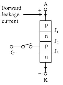
Ques.33. In the forward blocking mode, the middle junction (J2) has the characteristics of that of a:
- Inductor
- Capacitor✓
- Transistor
- None of these
A silicon controlled rectifier or semiconductor-controlled rectifier is a four-layer solid-state current-controlling unidirectional devices (i.e. can conduct current only in one direction). The whole operation of the thyristor is divided into three modes: Forward Blocking Mode The SCR is said to be forward biased when the anode is made positive with respect to the cathode. Due to this forward bias, the junction J1 and J3 are forward biased and J2 is reverse biased. Hence the forward voltage is to be held by junction J2. A very small current flows from anode to cathode. This current is called forward leakage current. This current is of the order of few milliamperes. In case this voltage is increased to high values, then the reverse biased junction J2 will experience an avalanche breakdown at a particular voltage called forward breakover voltage, VBO. As a result, the thyristor switches to conduction (ON) state. When the forward voltage is less than VBO, SCR offers high impedance in forward blocking mode. When the forward voltage reaches VBO, the SCR turns on. In forward blocking mode depletion layer J2 act as a dielectric and junction J1 and J3 acts as two plates. The SCR now behaves like a capacitor. Due to the space charges in the depletion region. The charging current of the capacitor is given as I = C dv/ dt where dv/dt is the rate of change of applied voltage and C is the junction capacitance. When the switch is suddenly closed dv/dt is large. Large charging current C dv/ dt flows through the SCR and the junction J2 breaks down. Therefore the SCR turns on without a gate signal. This method is not generally used since large charging currents may damage the device.
Ques.34. Conduction band and valence bands overlap in
- Conductor✓
- Semiconductor
- Insulator
- None of these
An energy band is a large group of orbitals whose energies are closely spaced and whose average energy is the same as the energy of the corresponding orbital in an individual atom. An energy band containing valence electrons is called the valence band. If the valence band is partially filled it requires very little added energy to excite a valence electron to a slightly higher energy orbital. Such a small increment of energy can be provided by applying an electric field, for example. The band with the next higher average energy above the valence band is called the conduction band. In a metal, the valence band and the conduction band overlap, so electrons can move freely from the valence band to the conduction band this explains the high electrical conductivity of metals. A substance with overlapping valence and conduction bands is an electrical conductor (or just conductor). When the conduction band is close in energy to the valence band, the electrons can absorb a wide range of wavelengths in the visible region of the spectrum. As the excited electrons fall back to their lower energy states, they emit their extra energy as visit light, producing the luster characteristic of metals. In a semiconductor, a narrow energy gap separates the valence band and the conduction band. At very low temperatures, electrons remain in the filled low energy valence band, and semiconductors are not good conductors. As temperature rise more electrons have enough energy to jump across the band gap into the conduction band, so conduction increases. A sufficiently large electric field also can provide the energy needed for electrons to jump the band gap. This property of semiconductors— switch from insulator to conductor with the application of an external electric field— the basis for the operation of transistors, the cornerstone of modern electronics. The energy-band theory also explains why some solids are electrical insulators (or just insulators), that is, substances that do not conduct electricity. In an insulator, there is a large band gap between the valence and conduction bands. Very few electrons have enough energy to move across the large gap from a filled lower energy band to an empty higher energy band, so no current flows through an insulator when an external electric field is applied.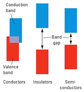
Ques.35. In the hydroelectric power station, Kaplan turbine is used for
- Medium head
- High head
- Low Head✓
- None of these
A turbine is a hydraulic machine which converts hydraulic energy into mechanical energy. Turbines are classified as given below: The impulse or Pelton wheel is generally used in plants with heads higher than 850 feet (260 meters), although some installations have lower heads. A reaction turbine is a type of turbine that develops torque by reacting to the pressure or weight of a fluid; the operation of reaction turbines is described by Newton’s third law of motion (Every action has an equal and opposite reaction). E.g of Reaction turbine is the Kaplan turbine, Propeller turbine, Francis turbine, Bulb turbine, Straflo, Tube turbine. Pelton is the high head turbine. Francis is the medium head turbine, while Kaplan is the low head turbine with an approximate height of 2 – 40 m,
Ques.36. Depending upon the voltage to be handled, switches may be broadly classified into
- Outdoor type
- Indoor Type
- Both outdoor and Indoor✓
- None of these
SWITCHGEAR DEFINITION:- Switchgear is a general term covering switching and interrupting devices that control, meter and protect the flow of electric power. or The apparatus used for switching controlling and protecting the electrical circuits and equipment is known as switchgear. Switchgear Equipment Switchgear covers a wide range of equipment concerned with switching and interrupting currents under both normal and abnormal conditions. It includes switches, fuses, circuit breakers, relays and other equipment. A brief account of these devices is given below. Switches:- A switch is a device which is used to open or close an electrical circuit in a convenient way. It can be used under full-load or no-load conditions but it cannot interrupt the fault currents. When the contacts of a switch are opened, an arc is produced in the air between the contacts. This is particularly true for circuits of high voltage and large current capacity. The switches may be classified into (i) air switches (ii) oil switches. The contacts of the former are opened in the air and that of the latter is opened in oil. SWITCHGEAR ACCOMMODATION It is necessary to house the switchgear in power stations and sub-stations in such a way so as to safeguard personnel during operation and maintenance and to ensure that the effects of the fault on any section of the gear are confined to a limited region. Depending upon the voltage to be handled, switchgear may be broadly classified into (i) Outdoor type. For voltages beyond 66 kV, switchgear equipment is installed outdoor. It is because, for such voltages, the clearances between conductors and the space required for switches, circuit breakers, transformers, and others equipment become so great that it is not economical to install all such equipment indoor. (ii) Indoor type. For voltages below 66 kV, switchgear is generally installed indoor because of economic considerations. The indoor switchgear is generally of metal-clad type. In this type of construction, all live parts are completely enclosed in an earthed metal casing.
Ques.37. During the transition time or turn on time
- The forward anode voltage is increased from 10% to 90% & the anode current decreases from 90% to 10% of the initial value
- The forward anode voltage is decreased from 90% to 10% & the anode current decreases from 90% to 10% of the initial value
- The forward anode voltage is decreased from 90% to 10% & the anode current increases from 10% to 90% of the initial value✓
- The forward anode voltage is increased from 10% to 90% & the anode current also increases from 10% to 90% of the initial value
Turn-ON Characteristics of Thyristor When the thyristor is forward biased and a positive gate pulse is applied between the gate and cathode, it will be turned ON. But there is a finite transition time to switch from forward OFF-state to forward ON-state for a thyristor. This finite transition time is known as turn-ON time. The turn-ON characteristics of the thyristor are shown in Fig. The turn-ON time tturn-on is the sum of the delay time td, rise time tr and spread time tp and it can be expressed as tturn-on = td + tr + tp Delay time td:- There is a time delay to turn on a device. The delay time td is the required time interval from initial anode current, i.e., forward leakage current to reach 10% of the final value of anode current (0.1IA) where IA is the final value of anode current. The delay time td can be measured from the instant of the gate current reaches 0.9Ig to the instant at which anode current reaches to 0.1IA where Ig is the final value of gate current and IA is the final value of anode current. The delay td can also be measured by the time interval during which anode voltage falls from VA to 0.9VA where VA is the initial value of anode to cathode voltage. This delay time can be decreased by applying high gate currents and high forward anode to cathode voltages. The delay time tat is a fraction of a microsecond. Rise time tr:– The rise time is the time interval during which the anode current increases from 10% to 90% of final anode current. During rise time the forward blocking OFF-state voltage decreases, the rise time tr: can be measured from the instant of 90% of forward blocking OFF-state voltage (0.9VA) to the instant at which forward blocking OFF-state voltage reaches to 0.1 VA. The rise time tr: can also be measured from the instant of the gate current reaches 0.9Ig to the instant at which gate current Ig where Ig is the final value of gate current. The rise time is inversely proportional to the amplitude of the gate current and its build-up rate. The rise time decreases when high and steep current pulse is applied to the gate of SCR. The value of tr depends on the nature of the anode circuit (R-L and R-C circuits). For example, in a series R-L circuit, the rate of rise of anode current is slow due to the presence of inductance L and rise time is more. In case of a series R-C circuit, the rate of rise of anode current is high and rise time is less. During rise time, turn-on losses in the thyristor are the highest due to high anode voltage and large anode current simultaneously occurring in the thyristor. As these losses occur only over a small conducting region, local hot spots may be formed and the de be damaged. Spread time tp:- The spread time is the time interval during which the forward blocking voltage falls from 10% of its value (0.1VA) to the ON-state voltage drop about 1 V to 1.5 V. The spread time can be defined as the time taken by the anode current to rise from 0.9IA to IA. During this time, the conduction spreads over the entire cross-section of the SCR cathode. The spreading time depends on the area of the cathode and gate structure of SCR. After spread time, SCR is completely turned on and final steady-state anode current flows through the device and the voltage drop across SCR is about 1 V to 1.5 V. The total turn-ON time of SCR is equal to 1 to 4 µs. The total turn-ON time depends on the anode circuit parameters and the amplitude of the gate current and its wave shape. With the increase of gate current, the turn-ON time will be decreased significantly. The amplitude of the gate current is 3 to 5 times of minimum gate current to trigger thyristor. During the design of the gate triggering circuit, the following conditions should be maintained: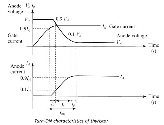
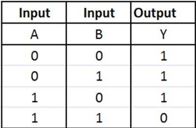
Ques.38. Which gate operation give high output when any one of its input is high?
- EX-OR Gate✓
- NAND Gate
- NOR GATE
- EX-NOR Gate
The exclusive OR gate has a high output only when an odd number of inputs is high. The figure shows a two-input exclusive OR gate (XOR) with the single output. When the input signals A and B are low, both AND gates have low outputs and hence the output of the OR gate Y is also low. If the input signal A is low and the input signal B is high, the upper AND gate have a high output and lower AND gate has a low output. As the upper AND gate has a high output, the output of the OR gate Y has a high output. Similarly, when the input signal A is high and the input signal B is low, the final output Y is high as the lower AND gate has a high output. If both the input signals A and B are high, both AND gates have a low output resulting is a final low output Y. The truth table for a two-input exclusive-OR gate as explained above is tabulated in Table Note:- Nand gate:- NAND produces a low output only if all the inputs a high. If any of the inputs is at low, then it produces a high output. Nor gate:- The logic operation of NOR-gate is such that a low output occurs when any of its inputs are high and output will be high only if all of its inputs are low. Ex-NOR gate:- These are special gates combination which provides logic 1 output when their inputs have the same log combinations. The output will be in state 1 only if both inputs are simultaneously high (or in state 1) or both Simultaneously low.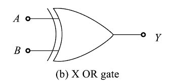
Ques.39. By using ______ false triggering of the SCRs by varying flux & noise is avoided
- F.A.C.L.F & C.B
- Shielded Cable & twisted gate leads
- Snubber circuit✓
- di/dt inductor in series with the gate terminal
Thyristor protection or SCR Protection The transient overvoltages can switch on the thyristor. In some cases, the thyristor can be damaged due to these transient voltages. These transient voltages are very common when the converter is having inductive loads. Snubber circuit: The thyristors can be protected against transient voltages by an RC network This RC network is connected in parallel across the thyristor. It is called snubber circuit. The Fig. shows snubber(RC) circuit. The resistance has the value of few hundred ohms. Whenever there is a large spike or voltage transient across the thyristor, it is absorbed by the RC circuit. The RC circuit (snubber) acts as a lowpass filter for this voltage transient.A low-pass filter (LPF) is a filter that passes signals with a frequency lower than a certain cutoff frequency and attenuates signals with frequencies higher than the cutoff frequency. The resistance has normally low value so that the transient is absorbed by the capacitor quickly. Thus the thyristor is protected against voltage transients. The RC snubber circuit very commonly used for protection of thyristors against transient voltage High-frequency voltage spikes).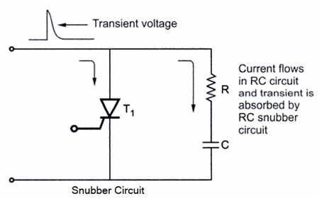
Ques.40. The forward dv/dt rating of an SCR:-
- Decrease with the decrease in the RMS value if forward anode-cathode voltage
- Decrease with the increase in the junction temperature
- Increase with an increase in the junction temperature✓
- Increase with the decrease in the RMS value of forward anode-cathode voltage
dv/dt is the rate of change of anode to cathode voltage with respect to time. The dv/dt rating of a thyristor indicates the maximum rate of rise of anode voltage that will not trigger the device without any gate signal. If the rate of rise of forward voltage is higher than the specified maximum value, it may cause switching fro the OFF-state to the ON state. The mechanism for this phenomenon can be explained in terms of internal capacitance that the thyristor exhibits. Whenever the SCR is in forward blocking state, only forward leakage current flows through the SCR. In such state, an equivalent internal capacitor is formed inside the SCR from an anode to gate and gate to cathode. Fig. shows such an internal circuit. Whenever the voltage applied across the SCR changes rapidly, a transient current flows through the SCR This transient current flows due to rapid voltage variations (dv/dt) and internal capacitance. This current adds to the forward leakage current. And hence the SCR turns on even if anode to cathode voltage (VAK) < Break over voltage (VBO) or gate drive is not applied. The dv/dt turn-on makes false triggering (unwanted) of the SCR. It is never used for triggering. Every SCR has dv/dt rating. It is expressed in volts per microseconds (V /μs). The voltage variations across the SCR must be kept less than the permissible value of dv/dt to avoid false triggering. Normally a small resistance is connected between gate and cathode to avoid false triggering of SCR due to dv/dt. Hence when voltage across the device is increased, charges flow through it in a manner analogous to tile charging current of a capacitor (i = C dv/dt ). The greater the rate of rise of applied voltage, the greater will be this flow of charges. As the rate of rise is increased. Efficient charges will eventually flow to act as a gate current o turn-on the SCR even without any positive gate signal. Effect of temperature on dv/dt rating. The dv/dt rating of SCR depends upon the temperature. dV/dT decreases with increasing temperatures for the semiconductor diodes. As temperature increases, the forward bias voltage of a diode decreases. For every 1° increase in temperature, the forward voltage decreases approximately by 2 mV. An increase in temperature causes an increase in intrinsic carrier density, a decrease in band gap cause an increased value of diode current. All these factors lead to a net result that is with an increase in temperature, the diode current increases. An increasing diode current leads to power dissipation in the diode, which ultimately leads to further increase in temperature.